The ten pins
VCC, GND, SCL, SDA, ADDR, ALERT, A0, A1, A2, A3, printed in that order on both faces of the board. Four of those pins already have a resistor fitted, and knowing which four explains most of what the board does before you write any code.
Ten holes, one row
Every pin is on one edge, at the usual 2.54 mm spacing, with the headers already soldered. The board is 17.2 × 27.9 mm, so it straddles a breadboard's centre channel with the whole row on one side and nothing opposite it.
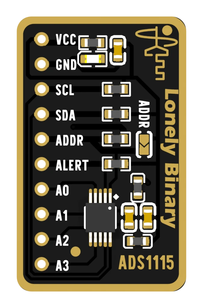
What is already fitted
Four of the ten pins arrive with a resistor on them, and two of those decide how the board behaves out of the box.
- SCL and SDA each have a 10 kΩ pull-up to VCC. An I²C bus needs pull-ups somewhere, and this board brings its own, so a single module works with nothing added.
- ALERT has a 10 kΩ pull-up too, and needs it more than the others. That pin is open drain — the chip can pull it to ground and cannot push it up — so without a resistor it would never read high at all.
- ADDR has a 10 kΩ pull-down, to ground. That is why the board answers at 0x48 the first time you scan for it, with nothing connected to that pin.
Plus the parts that are not on a pin: two ferrite beads separating the chip's supply and ground from the header's, three capacitors around the chip, and a red LED across the supply.
Reading the back
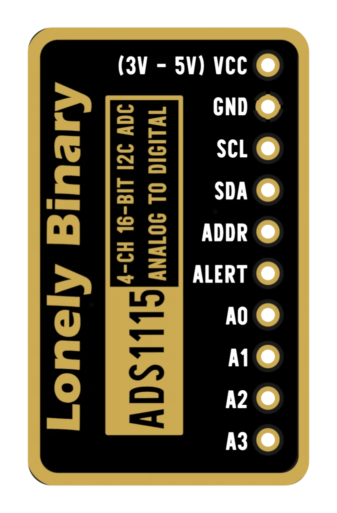
The supply range printed on the back is narrower than the datasheet's on purpose. The chip works down to 2.0 V, but the whole point of the board is measuring things, and the supply is also the ceiling on what the analog inputs may see. There is not much use in a converter that can only take 2 V.
The four that matter
A0 to A3 are the only pins on this board with nothing between them and the chip. No resistor, no capacitor, nothing but a track. That is deliberate — anything in the way is an error in the reading — and it is also the reason to be careful with them. There is no protection on this board beyond the chip's own diodes, and those give up about 0.3 V past the supply rail.
Wire the supply first. Then worry about what goes on the inputs.
When it does not work
The end nearest the ADDR solder pad and furthest from the chip, and it is labelled. Both faces of the board print all ten names beside their holes, so there is no counting to do — read the silkscreen. The back also prints the supply range and what the board is.
No, and it is an unlucky collision. A0 here is analog input 0 on the ADS1115, reached by setting the multiplexer and reading over I²C. A0 on an Uno is one of that board's own analog pins. Nothing connects them unless you wire them together, and there is no reason to.
Not in software. It is wired straight across the supply through a 5.1 kΩ resistor and draws under a milliamp, which is more than the chip itself uses but negligible next to any microcontroller. On a battery project where that matters, the resistor can be removed with a soldering iron.
Ferrite beads, 600 Ω at high frequency and close to a short at DC. One is in the supply and one is in the ground, so the chip's own supply and ground are isolated from whatever noise is travelling along the wires to your microcontroller. They are the reason this board reads more quietly than a bare chip on a breadboard.
Four wires in the order they have to go on, and the address that proves it worked.
Power, and a first scan →Edit this page — content/books/ads1115/the-ten-pins.mdx
Questions about this product
See what other owners have asked, and read their solutions.
This page covers several products. Choose yours to see the right discussions.
Discuss this article
Ask about this page. The answer stays here, on the page it belongs to, for whoever hits the same wall next.