Specifications
| In the 3-pack | 3 ADS1115 modules, headers fitted |
|---|---|
| In the 6-pack | 6 ADS1115 modules, headers fitted |
| Converter | Texas Instruments ADS1115IDGSR, 16-bit delta-sigma, with an internal reference and oscillator. VSSOP-10 package |
| Inputs | 4 single-ended, or 2 differential pairs, or 3 measured against A3 as a common point. One converter behind a multiplexer |
| Supply | 2.0 V to 5.5 V per the datasheet; the board prints 3 V to 5 V. About 150 µA converting continuously, 0.5 µA between single-shot conversions |
| Input range | Six full-scale ranges from ±6.144 V to ±0.256 V, giving 187.5 µV to 7.8125 µV per count. An analog input must still stay between ground and the supply |
| Resolution | 16 bits across ±FSR. A single-ended reading against ground uses the positive half only, so it returns 0 to 32767 |
| Data rate | 8, 16, 32, 64, 128, 250, 475 or 860 samples per second. Conversions settle in one cycle, so the conversion time is 1 / rate |
| Noise | One count peak-to-peak up to 128 SPS in every range, rising to about 14 bits noise-free at 860 SPS in the narrowest range |
| Addresses | 0x48 as shipped, 0x49 with the ADDR solder pad bridged — so 2 modules per I²C bus. TI's other two addresses need the board's 10 kΩ pull-down on ADDR removed first |
| On-board parts | 10 kΩ pull-ups on SCL, SDA and ALERT; a 10 kΩ pull-down on ADDR; two 600 Ω ferrite beads isolating the chip's supply and ground; 10 µF and 100 nF decoupling; a power LED |
| ALERT pin | Open drain, pulled up on the board. A threshold comparator with hysteresis, a window comparator, or an 8 µs pulse at the end of every conversion |
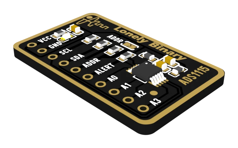
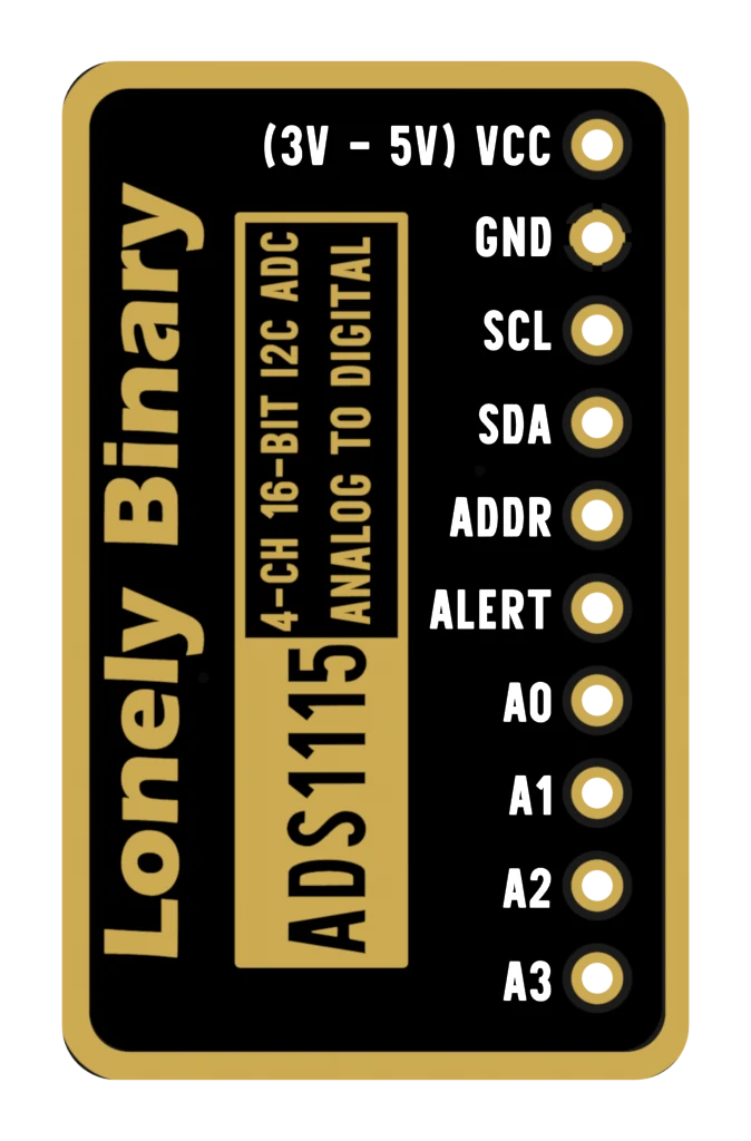
| Pins | VCC, GND, SCL, SDA, ADDR, ALERT, A0, A1, A2, A3 in that order, 2.54 mm pitch, headers fitted. Board 17.2 × 27.9 mm |
What it does
A microcontroller's analog input divides its whole range into steps, and the step never gets smaller when your signal does. An ESP32 divides about 3.1 V into 4096 of them, which is fine for a knob and useless for a thermocouple.
The ADS1115 moves its range down to fit the signal instead. Six ranges from ±6.144 V to ±0.256 V, sixteen bits spent inside whichever one you choose, and its own voltage reference and oscillator three millimetres from the inputs rather than on a die shared with a Wi-Fi radio.
It costs two GPIO pins that the I²C bus was probably already using, and a few milliseconds per reading. It is a precision part, not a fast one — 860 conversions a second at the very top.
The two boxes
Both boxes hold the same board — the 3-pack and the 6-pack differ only in how many. The converter is a genuine Texas Instruments ADS1115IDGSR, and the board adds what a bare chip on a breadboard does not have: pull-ups on the bus, a pull-down that fixes the address, two ferrite beads isolating the chip's supply and ground from the wires running back to your microcontroller, and three decoupling capacitors.
Which range for which signal
| Your signal reaches | Range | One count |
|---|---|---|
| up to 3.3 V, board on 3.3 V | ±4.096 V | 125 µV |
| up to 5 V, board on 5 V | ±6.144 V | 187.5 µV |
| up to 2 V | ±2.048 V | 62.5 µV |
| up to 1 V | ±1.024 V | 31.25 µV |
| a few hundred millivolts | ±0.512 V | 15.625 µV |
| tens of millivolts | ±0.256 V | 7.8125 µV |
Anything above your supply is not a range question. It needs two resistors in front of the pin, and measuring a 12 V battery works one through start to finish.
Wiring, in four lines
- VCC to 3.3 V — or 5 V, but only if your microcontroller is a 5 V board.
- GND to ground, and to the ground of whatever you are measuring.
- SDA and SCL to the microcontroller's I²C pins.
- Then the signal to A0, with its return on GND or on A1.
Leave ADDR and ALERT unconnected. Both already have a resistor holding them where they need to be, and a wire in either hole at the start can only make things worse.
A scan should find the board at 0x48. That single line of output proves the supply, the ground and both bus wires at once.
Where to start
The handbook below is eleven short articles with a working figure in each. If you read one, read the gain is a range, not an amplifier — it is the difference between a good reading and a damaged chip. If your readings are already wrong, when the reading is wrong sorts the four common faults by the shape they make on a plot.
When it doesn’t work
- Can it measure 6.144 V if I select the ±6.144 V range?
- No, and this is the mistake that costs people chips. The range setting decides what one count is worth, and nothing else. The voltage a pin may actually see is the supply — TI's absolute maximum is 0.3 V above VDD, past which the protection diodes conduct and the part can be permanently damaged. On a 3.3 V board the ±6.144 V range simply throws away half its codes. Anything bigger than your supply needs a two-resistor divider in front of it.
- Is it really 16 bits?
- Across a differential measurement, yes. Against ground, no: the chip always converts a difference and always returns a signed number, and these inputs cannot go below ground — so the negative half of the scale is unreachable and a single-ended reading runs 0 to 32767. Fifteen bits and a sign bit that is always zero. The step size is unchanged; it is the span that halves.
- How many of these can I put on one bus?
- Two. The board fits a 10 kΩ pull-down on ADDR, which is what makes it answer at 0x48 out of the box, and bridging the solder pad ties ADDR to VCC for 0x49. TI's other two addresses need ADDR wired to SDA or SCL, and that pull-down would then hold the bus line at half the supply — neither a high nor a low. Removing the resistor opens them up; short of that, use the microcontroller's second I²C bus for boards three and four.
- Why are my readings noisy?
- Check the data rate first. Up to 128 samples per second the noise is one count in every range, which is as quiet as the chip's own resolution. At 860 SPS it is several counts, and in the narrowest range under fourteen bits are real. Drop to 8 or 16 SPS for anything that does not move fast, and average in the sketch if you need both speed and quiet.
- Do I need pull-up resistors on the bus?
- Not for one or two of these — each board brings a 10 kΩ on SDA and on SCL. Two boards make 5 kΩ, which is still comfortable. A crowded bus with several other modules all contributing their own pull-ups can end up pulled harder than devices can drive against, which is worth measuring if a busy bus starts misbehaving.
- Can I power it from 5 V and use it with an ESP32?
- Not directly. The pull-ups go to VCC, so a 5 V module puts 5 V on SDA and SCL when the bus is idle, and a 3.3 V microcontroller should not have that on its pins. Either run the module from 3.3 V and divide your signal down, or put a level converter in the bus. The first is almost always the better answer.
- My unused inputs read random numbers.
- That is correct behaviour. Nothing on this board holds A0 to A3 anywhere — no pull-up, no pull-down — so an unwired input floats and picks up the mains field in the room. It does not affect the channels you are using. Tie unused inputs to GND if the numbers bother you.
- Which library should I use?
- ADS1X15 by Rob Tillaart, from the Arduino Library Manager, is the one the handbook's sketches use. Adafruit's ADS1X15 library works too. Worth knowing: Rob Tillaart's library starts at gain 0, which is the ±6.144 V range, so a sketch that never calls setGain is using the coarsest setting there is.