The two boards
One block with one channel and one wide board with three. They share pull-ups, address pads and wiring habits, fit different shunts — 100 milliohms and 50 — and their four-pin headers disagree about which of SDA and SCL comes first.
Same instrument, two resistors
Much is identical on the two boards: 10 kΩ pull-ups on both bus lines, solder pads to move the address, a red power LED off the supply rail through 5.1 kΩ, and a ground shared between the rail being measured and the microcontroller.
What differs is the chip, and the resistor that goes with it. The TK119 carries one INA219, which has a gain stage in front of its converter and so four current ranges you pick in software, on a 100 milliohm shunt. The wide board carries one INA3221, which has three channels and no gain stage, so one range for all three — and because that one range is narrow, each channel gets a 50 milliohm shunt to reach 3.28 A. The back of the board prints exactly that.
The header, which is the trap
| Pin 1 | Pin 2 | Pin 3 | Pin 4 | |
|---|---|---|---|---|
| TK119 | GND | 3V3 | SCL | SDA |
| INA3221 | GND | VCC | SDA | SCL |
Four wires either way, and the last two swap. If you wire one board, get it working, then move the same four jumpers onto the other, the bus goes silent and a scan reports nothing. No damage — I²C lines are open drain and the pull-ups are the same on both — but nothing at all to tell you why.
The habit worth forming with these two boards is reading the silkscreen every time. It is printed on the front of both.
What the INA3221 adds
Three things beyond the extra channels.
Four alert pins, brought out on the 14-pin header and marked CRI, WAR, TC and PV. Critical and warning compare the current against limits in hardware, so the board notices a problem whether your sketch is looking or not — and each of those two already has a red LED wired to it, so it also notices visibly.
A cuttable pull-up pad, marked I2C PULL-UP. Cut it and the board's two 10 kΩ resistors come off the bus, which is what you want when several devices share the wires and their pull-ups add up.
A three-way ground terminal, so three channels' negatives can each have a screw of their own rather than sharing one.
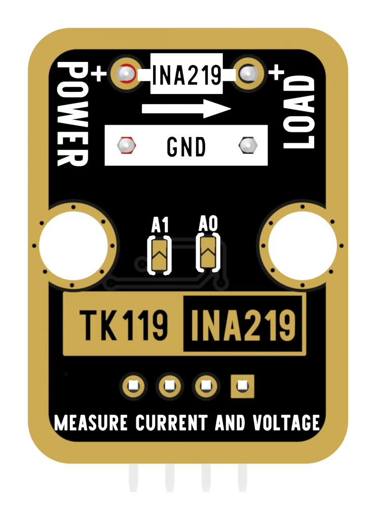
What the TK119 adds
Two things, and they make it the better first board. The range is yours to choose, and the steps are fine. The INA219's gain setting spans ±40, ±80, ±160 or ±320 millivolts, which across 100 milliohms is ±0.4 to ±3.2 amps — so the same block can watch an LED strip and a motor starting — and every count is 0.1 mA, against 0.8 mA on the INA3221.
It also has a power register, so watts arrive without arithmetic. The INA3221 has none, and you multiply.
When it does not work
Check the last two pins of the header against the silkscreen, not against your wire colours. The TK119 reads GND, 3V3, SCL, SDA and the INA3221 reads GND, VCC, SDA, SCL, so the two are the other way round. Swapped SDA and SCL do no damage at all — the bus simply never completes a transaction, which is indistinguishable from a dead board until you look.
They both leave the factory at 0x40, because every address pin has a 10 kΩ pull-down fitted. Two devices at one address on one bus is two devices neither of which works. Bridge the INA3221's I2C ADDR pad to move it to 0x41, or one of the TK119's two pads on the back. See the next page.
It does, deliberately: pins 4 to 9 are the same six nets as the three channel terminals, so a channel can be wired with a jumper instead of a screwdriver. Do not use both for one channel — two paths in parallel across one shunt means only some of the current goes through the resistor, and the reading is low by whatever fraction took the other route.
The TK119 is 22.4 × 30.4 mm and the INA3221 is 48.0 × 30.6 mm, both with two mounting holes. The screw terminals overhang the edge of the board slightly and stand about 10 mm tall, so allow for them when measuring a case. The figure above draws both to scale.
Edit this page — content/books/inaset/the-two-boards.mdx
Questions about this product
See what other owners have asked, and read their solutions.
This page covers several products. Choose yours to see the right discussions.
Discuss this article
Ask about this page. The answer stays here, on the page it belongs to, for whoever hits the same wall next.