Specifications
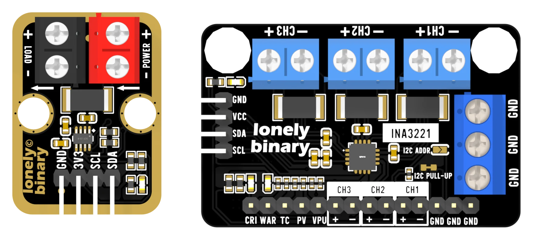
| Boards | 2 monitors, sold separately or as a set: the TK119 with one INA219, and a wide board with one INA3221. Different shunts, the same wiring habits |
|---|---|
| Channels | 4 in total — 1 measured channel on the TK119 and 3 on the INA3221, each with its own shunt |
| Shunt | TK119: 100 mΩ, 1%, 2 W, Yageo PT2512FK-7W0R1L. INA3221: 50 mΩ on each of the three channels. Both 2512 packages, in the positive wire between the supply and the load |
| Current range | TK119: ±0.4, ±0.8, ±1.6 or ±3.2 A, chosen in software. INA3221: ±3.28 A per channel, fixed. Above it the reading sits at full scale and stops moving |
| Resolution | One count is 0.1 mA on the TK119 (10 µV of shunt register) and 0.8 mA on the INA3221 (40 µV across 50 mΩ). Neither can see a sleeping microcontroller |
| Bus voltage | 0 to 26 V on both, measured from the load side of the shunt down to the board's own ground. 26 V is an absolute maximum, not a recommendation |
| Supply | 3 to 5.5 V for the INA219, 2.7 to 5.5 V for the INA3221 — the chip's own supply, separate from the rail being measured. The TK119's hole is silkscreened 3V3 and the INA3221's is silkscreened VCC on the front and 3-5V on the back |
| Isolation | None. On both boards the negative screws, the GND header pins and the chip's ground are one net, so the rail being measured must share a ground with the microcontroller reading it |
| I²C address | 0x40 out of the box on both. The TK119 has A1 and A0 pads and so four addresses — 0x40, 0x41, 0x44 and 0x45; the INA3221 has one A0 pad and so two, 0x40 and 0x41 |
| Pull-ups | 10 kΩ on SDA and SCL on both boards, to their own supply rail. The INA3221's pair runs through a cuttable pad marked I2C PULL-UP; the TK119's does not |
| Bus levels | Set by whatever you put on the supply pin, because the pull-ups pull to it. SDA is rated to 6 V on both chips; SCL only to the supply plus 0.3 V, so run the board from the same rail as your microcontroller's logic rather than mixing 3.3 and 5 V |
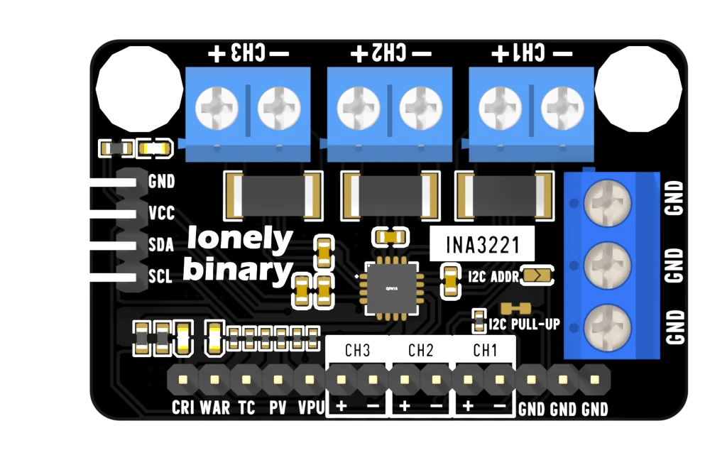
| Alerts | 4 open-drain pins on the INA3221 — critical, warning, power-valid and timing control — brought out on the 14-pin header, with an LED already fitted on critical and on warning. None on the TK119 |
| Headers | TK119: a 4-pin right-angle header printed GND, 3V3, SCL, SDA. INA3221: a 4-pin right-angle header printed GND, VCC, SDA, SCL, plus a 14-pin straight header carrying all three channels and the four alerts |
| Terminals | KF301-5.0 screw terminals on 5 mm pitch. Two 2-way on the TK119 (POWER and LOAD), three 2-way and one 3-way ground on the INA3221 |
| Power LED | Red, from the supply rail through 5.1 kΩ. One on the TK119, and one of three on the INA3221 — the other two are the critical and warning alerts |
| Size | TK119 22.4 × 30.4 mm, INA3221 48.0 × 30.6 mm, two mounting holes each |
What they do
Both boards put a small resistor in the positive wire between a supply and a load — 100 mΩ on the TK119, 50 mΩ on each INA3221 channel — and read the millivolts that appear across it. Ohm's law turns those millivolts into current. Each board also measures the voltage on the load side of the resistor, so it can tell you what the load is actually getting.
That is the whole instrument. Everything else on either board is a supply pin, two pull-up resistors, an address pad and — on the INA3221 — four alert pins that compare the reading against limits in hardware.
Which board
| TK119 INA219 | INA3221 | |
|---|---|---|
| Channels | 1 | 3 |
| Shunt | 100 mΩ | 50 mΩ per channel |
| Current range | ±0.4 to ±3.2 A, chosen in software | ±3.28 A, fixed |
| One count | 0.1 mA | 0.8 mA |
| Power in hardware | Yes, a register | No, multiply it yourself |
| Alerts | None | Critical, warning, power-valid, timing control |
| Addresses | 4 | 2 |
| Reads current both ways | Yes | Yes |
Both reach about 3.2 A, by opposite routes. Reach for the TK119 when there is one rail and the current might be large or might be small — it is the one whose range you can move, and its steps are eight times finer. Reach for the INA3221 when there are three rails, or when you want the board itself to notice a problem while your sketch is busy.
The header
The two boards are wired alike in every respect except one, and it is the one that costs an evening:
| Pin 1 | Pin 2 | Pin 3 | Pin 4 | |
|---|---|---|---|---|
| TK119 | GND | 3V3 | SCL | SDA |
| INA3221 | GND | VCC | SDA | SCL |
Four wires either way, and the last two swap. Nothing is damaged by getting it wrong — the bus simply goes quiet.
Wiring, in four lines
- GND → your board's GND. Always first, and it is the same net as both negative screws.
- 3V3 (TK119) or VCC (INA3221) → the same rail your board's logic runs at, 3 to 5.5 V.
- SCL and SDA → your board's I²C pins. Check which order the board prints them in.
- The supply into POWER + / CHn +, the load out of LOAD + / CHn −, with the negatives in the remaining screws.
Then scan the bus. Both boards answer at 0x40 with nothing soldered.
Where to start
The handbook below is written for somebody who has not measured current before. It starts with what a shunt is and why these ones are a tenth and a twentieth of an ohm, and it ends with two working sketches and four meter readings that tell you whether either board is wired right.
The TK119's own reference page — the pinout, the quick wiring, the example in both languages — is where every other TinkerBlock part's is, on the blocks shelf.
When it doesn’t work
- Why do the two boards use different resistors?
- Because only one of the chips has a gain setting. The INA219 can stretch its input to ±320 mV, so the TK119 keeps a 100 mΩ resistor and still reaches 3.2 A. The INA3221's input is fixed at ±163.84 mV, which would stop at 1.64 A on 100 mΩ — so the INA3221 board fits 50 mΩ and reaches 3.28 A, the number printed on its back. The cost is a coarser step: 0.8 mA per count on the INA3221 against 0.1 mA on the TK119.
- Can I use these with a 5 V Arduino?
- Yes, with one rule: feed the board the same rail your microcontroller's logic runs at. Both chips run from 3 to 5.5 V, and the 10 kΩ pull-ups on the board pull the bus to whatever you put on its supply pin — so a 5 V Uno gets 5 V bus levels and a 3.3 V ESP32 gets 3.3 V, with no converter in between. Mixing the two is the thing to avoid, and in one direction it is an absolute-maximum violation rather than a nuisance: SDA is rated to 6 V on its own, but SCL is only rated to the supply plus 0.3 V, so a 5 V clock into a board running on 3.3 V is over the limit.
- Do I need to swap SDA and SCL between the two boards?
- Yes. The TK119's four-pin header reads GND, 3V3, SCL, SDA and the INA3221's reads GND, VCC, SDA, SCL, so the last two are the other way round. Moving a set of jumpers straight from one board to the other swaps the bus, and an I²C scan then finds nothing at all — which looks exactly like a dead board. Read the silkscreen rather than the wire colours.
- Which screw does the supply go in?
- On the TK119, the red terminal marked POWER; the load goes on the black one marked LOAD, and the arrows printed between them point the way the current flows. On the INA3221, each channel's + screw goes to its supply and the − screw goes to the load, and the separate three-way terminal is ground. Wired backwards, both boards still work — the current simply comes out negative and the voltage they report is the supply's rather than the load's.
- Can I measure a battery's negative wire instead?
- Not on these boards. Both are high-side monitors: the shunt is in the positive wire, and the board's own ground is the same net as both negative screws. Putting the shunt in the return path would connect the load's ground to your microcontroller's through the shunt, which shorts it out. Low-side sensing is a real technique and the INA219 chip supports it — a board wired for it is a different board.
- Why can it not see my ESP32 sleeping?
- One count is 0.1 mA on the TK119 and 0.8 mA on the INA3221, and the fixed zero-point error is worth about ±1 mA and ±1.6 mA respectively. A sleeping ESP32 draws tens of microamps — less than one count on either board, sitting under an error many times larger. These boards are for watching a rail at work, not for measuring sleep current — that needs a meter with a microamp range.
- Do they measure power as well?
- The INA219 does it in hardware: it has a power register, and a library reads watts straight out of it. The INA3221 has no power register at all — you read the bus voltage and the current for a channel and multiply them yourself, which is one line and exactly as accurate.