
The shield: twelve sockets, one rule
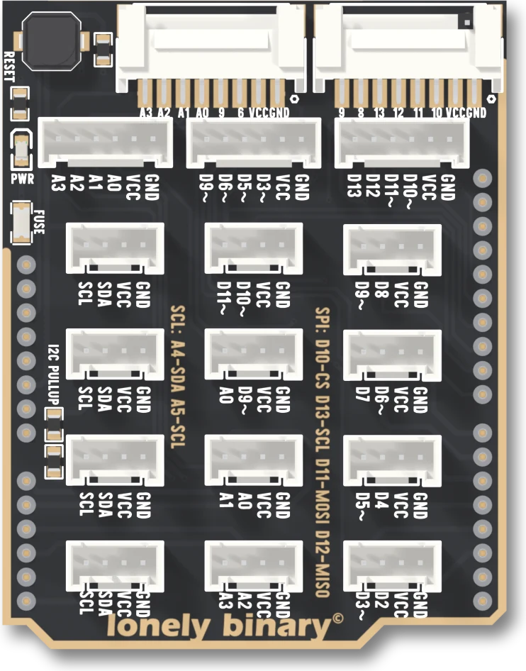
The shield turns the UNO's header strips into sockets. Every 4-pin socket carries GND, 5 V and two UNO pins, and a module's signal is on the socket's fourth pin: the second of the two pins printed beside it. The D2/D3 socket puts a module on D3. The rest of this page is what follows from that, and the few parts on the shield besides sockets.
Unplug the USB cable before you plug, unplug or move anything. Every socket carries 5 V, and a plug pushed in at an angle can touch the wrong pins on the way in.
Seating the shield
Do it with the USB cable out. Line the shield's outline up with the UNO's, check that every pin on its underside is straight and over its hole, and press down evenly until the shield sits flat on the UNO's header strips.
A bent pin is the one thing that goes wrong here. It folds under the shield instead of going into its hole, the shield still looks seated, and that one UNO pin never reaches its sockets. If it is the 5V pin, nothing lights; if it is a signal pin, one socket is dead and the rest work. Straighten it with fingers or flat pliers before trying again. Lift the shield off by rocking it gently along its length, not by prying up one corner.
The one rule
Every TinkerBlock module in this kit has a four-pin header: GND, VCC, an NC pin wired to nothing, and SIGNAL. Every 4-pin socket on the shield is GND, 5 V and two UNO pins, in the same order, and the cable joins pin to pin. So a module's SIGNAL lands on the socket's fourth pin, which is the second of the two UNO pins printed beside it.
Pick a socket and its fourth pin lights. That pin is where the module is. The third pin reaches the module's NC pin, so it does nothing while a kit module is plugged in.
| Socket | A module is on | PWM | Analogue |
|---|---|---|---|
| D2/D3 | D3 | yes | |
| D4/D5 | D5 | yes | |
| D6/D7 | D7 | ||
| D8/D9 | D9 | yes | |
| D10/D11 | D11 | yes | |
| D9/A0 | A0 | yes | |
| A0/A1 | A1 | yes | |
| A2/A3 | A3 | yes | |
| SDA/SCL, four of them | SCL, which is A5 | (yes) |
So the 4-pin sockets reach eight pins for single-signal modules: D3, D5, D7,
D9, D11, A0, A1 and A3. Four of them can fade an LED or set a buzzer's
volume with analogWrite, because D3, D5, D9 and D11 are among the UNO's
six ~ pins. Three take an analogue module.
D7 is digital only.
The rule costs one mistake, which every beginner makes once: reading the
first printed pin. The XL LED in the D2/D3 socket with pinMode(2, OUTPUT)
in the sketch stays dark, and nothing is wrong with either.
One UNO pin, several sockets
The shield does not give each socket pins of its own. It wires the UNO's pins out to several places, so the same wire turns up more than once, which the figure lights in amber. A0 is the D9/A0 socket's fourth pin and the A0/A1 socket's third; D9 is the D8/D9 socket's fourth pin and the D9/A0 socket's third. With kit modules that is harmless, because a third pin always meets an NC. It stops being harmless when two modules' signals share a wire, and the place that happens is the I2C sockets.
The I2C sockets and their pull-ups
The four sockets on the left are the same two wires four times: SDA, which is A4, and SCL, which is A5. I2C devices share those two wires and tell each other apart by address, so four I2C modules can sit side by side. The shield also pulls SDA and SCL up to 5 V through 4.7 kΩ each, the two resistors printed I2C PULLUP, because I2C needs a pull-up on both lines and many modules do not bring their own.
A single-signal module plugged in there is on SCL, and the pull-up is now part of its circuit:
- An input module reads differently. The push button holds its pin LOW with a 10 kΩ pull-down. Against 4.7 kΩ up, released, the pin sits at about 3.4 V, above the 3.0 V the UNO is sure to read as HIGH, so it reads pressed whether it is or not. An analogue sensor's reading is pulled towards 1023.
- An output module may switch on by itself. The IR transmitter's SIGNAL goes into a transistor through 1 kΩ. Until the sketch drives A5 LOW, the pull-up pushes about 0.75 mA into it, which is enough to turn the transistor on.
- Four modules there are on one pin. All four sockets put a module on SCL.
That is why only the IR transmitter goes there in this kit, and only in the
last chapter, where the sockets run out: its lab drives the pin from
setup() on.
The 6-pin and 8-pin sockets
| Socket | Pins after GND and 5 V | For |
|---|---|---|
| 6-pin, top right | D10, D11, D12, D13 | SPI: D10 CS, D11 MOSI, D12 MISO, D13 SCK |
| 6-pin, top middle | D3, D5, D6, D9 | four PWM pins |
| 6-pin, top left | A0, A1, A2, A3 | four analogue inputs |
| 8-pin, top edge left | D6, D9, A0, A1, A2, A3 | two PWM pins and four analogue inputs |
| 8-pin, top edge right | D10, D11, D12, D13, D8, D9 | SPI plus D8 and D9 |
They are for modules with wider headers, and none of the twelve in this kit uses them. Their pins are the same wires as the 4-pin sockets', so a module in a wide socket shares pins with whatever is in the small ones.
The SPI legend on top of the shield reads D13-SCL. It is a misprint: D13
is SCK, SPI's clock, and the underside prints 13 (SCK) correctly. SCL is
I2C's clock and lives on A5.
Power: the fuse and the PWR lamp
The sockets' 5 V is the UNO's 5V pin, through a resettable fuse on the shield marked FUSE (an nSMD100, which holds about 1 A). A short in a module or a cable heats it, it cuts the current until the short is gone and it has cooled, and then it conducts again by itself. On USB the UNO's own 0.5 A fuse is in the same path and is the lower of the two, so a short on a socket often puts out the UNO's ON lamp as well.
The PWR lamp, through a 1 kΩ resistor, sits on the sockets' side of the fuse. Lit, the sockets have 5 V. The UNO's ON lamp lit and PWR dark means the 5 V stops at the shield: a pin out of its hole, or a tripped fuse.
The reset button
The shield covers the UNO's own reset button, so it has one of its own, top
left, wired to the UNO's RESET pin. Pressing it restarts the sketch from
setup(), exactly as the button underneath would.
When it does not work
The sketch names the first of the two pins printed beside the socket. A module's signal is on the second: D2/D3 is D3, D4/D5 is D5, A0/A1 is A1, A2/A3 is A3. Change the number in the sketch, or move the module to the socket whose second pin it names.
The 5 V reaches the UNO but not the sockets. Either a shield pin missed its hole, or the fuse has tripped on a short in a module or cable. Unplug the USB cable, pull every module, reseat the shield, wait a minute for the fuse to cool, and plug in with no modules. Add them back one at a time.
The shield's 4.7 kΩ pull-up on SCL fights the button's own 10 kΩ pull-down, and released the pin sits at about 3.4 V, which the UNO reads HIGH. Plug the button into a digital socket; on this kit, D6/D7.
A misprint on the top. D13 is SPI's SCK, the clock, and the underside prints it correctly as 13 (SCK). SCL is I2C's clock, which is A5. Nothing in this kit uses the SPI socket.
Not a kit module. Their plugs have four pins and those sockets are wider, so the plug does not seat and the pins do not line up. The wide sockets are for modules with wider headers, such as an SPI display.
The first module on the shield, and a sketch that shows the one rule at work.
Lab: blink the XL LED →Edit this page — content/books/tkbu/the-shield.mdx
Questions about this product
See what other owners have asked, and read their solutions.
TinkerBlock UNO R3 Starter Kit, 12 Modules
Loading discussions…
Discuss this article
Ask about this page. The answer stays here, on the page it belongs to, for whoever hits the same wall next.