Six pins, in order
GND, VBUS, CC1, D−, D+, CC2, counting from the square pad. It is not the order anybody guesses, a configuration pin sits in the middle of it, and the labels are printed on both faces so you can check from the side you are soldering.
The row, top to bottom
Hold the board with the socket on your left and the pads on your right. The square pad is at the top, and it is GND. From there:
Nobody guesses this order. A configuration pin sits between the power and the data pair, and the second configuration pin is on the far side of the data pins rather than next to the first. There is a good reason — it follows the order the contacts appear inside the connector — but it means counting pads from a photograph is a bad way to wire this board. Read the labels.
The two you always wire
GND and VBUS. That is a working power supply, and for most projects it is everything this board is for.
Wire GND first. Every other voltage on the board is measured against it, and a circuit where the ground goes on last spends a moment with 5 V looking for a way home through a signal pin.
VBUS carries 5 V, not 3.3 V. On a development board it goes to the pin marked 5V or VIN, never to 3V3.
The two you leave alone
CC1 and CC2 are already done. Each has its 5.1 kΩ resistor to ground fitted on the board, and that resistor is what makes the socket work at all. They are brought out to the header so you can measure them — which turns out to be worth doing, and is what the sketch later in this book is for — but in ordinary use nothing connects to them.
The two you might
D− and D+ are the USB 2.0 data pair. If you only want power, leave them. If you want data, they need to stay together and stay short, and there is a chapter on what they can and cannot carry.
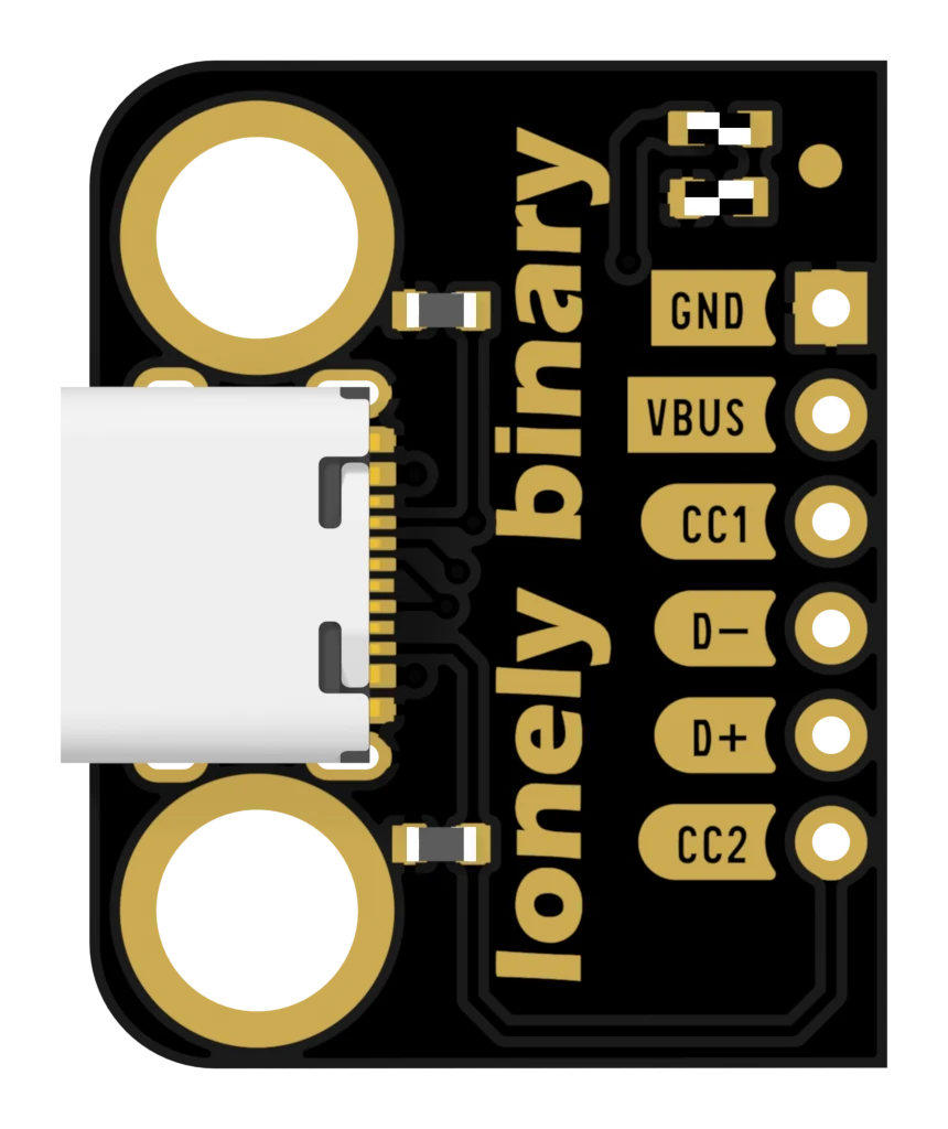
The pads are on a 2.54 mm grid, which is the spacing of every breadboard and every strip of the header in the bag.
When it does not work
VBUS is 5 V, and a 3V3 pin is the output of a regulator. Feeding 5 V backwards into it pushes current the wrong way through that regulator and past anything already on the 3.3 V rail. Move the wire to the 5V or VIN pin. If the board has neither, it wants 3.3 V and this socket is not the right way to feed it.
The square pad. Every other pad is round, and the square one is GND — at the end of the row nearest the top edge when the socket is on your left. Both faces are labelled, so if you have the board upside down for soldering you can still read the names.
No. They are already finished — each one has its 5.1 kΩ down to ground on the board, which is the whole handshake. They are brought out so you can measure them, or so you can build something cleverer later. Leaving both unconnected is the normal case.
That is exactly right and nothing is wrong. A cable connects only one of the two CC lines, chosen by which way up the plug went in. The one reading zero is the one the cable left open. Turn the plug over and the two readings swap.
Straight or right-angle, and the reason the choice is about where a plugged-in cable pulls.
Soldering the headers →Edit this page — content/books/usb-c-breakout/six-pins-in-order.mdx
Questions about this product
See what other owners have asked, and read their solutions.
USB-C Breakout Board, 12-Pack with 5.1 kΩ CC Resistors
Loading discussions…
Discuss this article
Ask about this page. The answer stays here, on the page it belongs to, for whoever hits the same wall next.