Specifications
| Driver | TI DRV8833 (DRV8833PWPR, exposed-pad TSSOP-16) |
|---|---|
| Supply (VM) | 2.7 – 10.8 V. Absolute maximum 11.8 V. Undervoltage lockout at 2.6 V or below, VM falling |
| Logic supply | None. The chip makes its own internal supply from VM |
| Channels | 2 H-bridges, each with two inputs and two outputs |
| Output current | 1.5 A RMS, 2 A peak per bridge (datasheet, VM 5 V, 25 °C, thermal limits observed). Less below VM 5 V |
| Overcurrent trip | 2 – 3.3 A, independent of the sense resistors. Retries after 1.35 ms |
| Sense resistors | R1 / R2 fitted at 0 Ω — the chip's current regulation is off |
| nSLEEP threshold | 2.5 V to read high, 500 kΩ pulldown in the chip. AIN1, AIN2, BIN1, BIN2: 2.0 V, 150 kΩ pulldowns. No pulls on the board |
| FLT | Open drain, no pull-up on the board. Low during an overcurrent trip or thermal shutdown |
| Power LED | Red, with 5.1 kΩ across VM. Lit whenever VM is present, asleep or not: about 0.6 mA at 5 V (worked out) |
| Connectors | None fitted. KF301 5.0 mm screw-block and 2.54 mm footprints on power and each motor; 8-pin 2.54 mm control header |
| Size | 22.5 × 27.5 mm, two Ø4.8 mm mounting holes 16 mm apart |
What it does
Two H-bridges in one package. Each takes two logic inputs and drives two output pads, so four GPIO pins give you two DC motors turning either way, or one bipolar stepper. Both inputs low coasts, both high brakes, one high turns the motor.
There is no logic supply pin. VM is the only supply, 2.7 to 10.8 V, and the chip makes its own internal supply from it. The absolute maximum is 11.8 V, so a nominal 12 V lithium pack fresh off the charger is already past it.
What ships in the box
The bare board, with the connectors loose: screw terminals and a header, to solder where your build wants them.
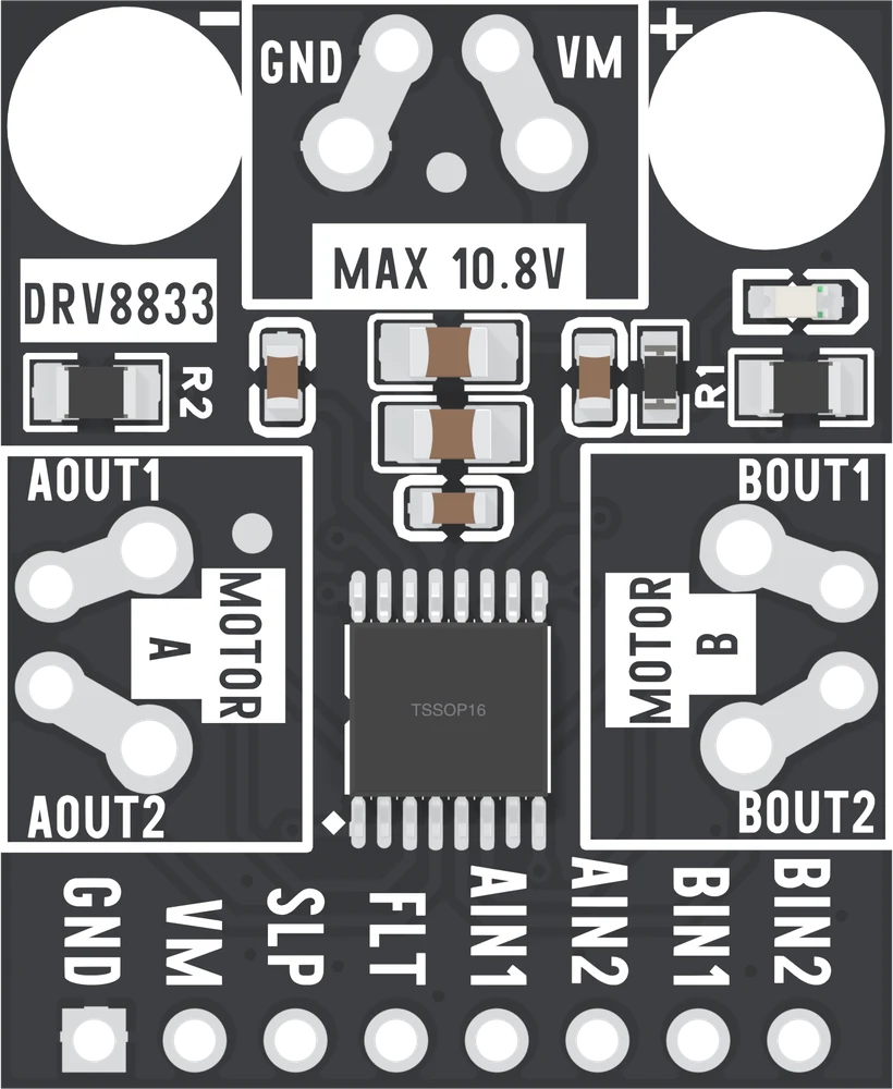
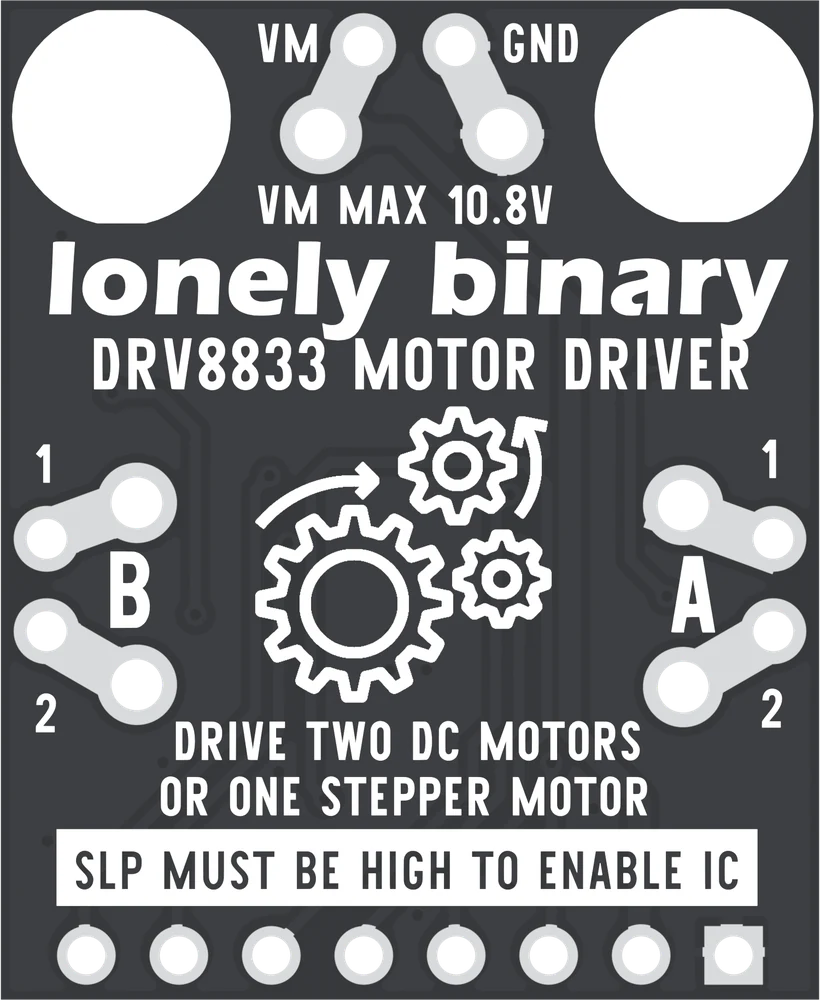
The front carries the pin names: GND and VM on the power terminal, AOUT1 above
AOUT2, BOUT1 above BOUT2, and the header's GND, VM, SLP, FLT, AIN1, AIN2, BIN1,
BIN2. The back carries VM MAX 10.8V, SLP MUST BE HIGH TO ENABLE IC, and a 1
above a 2 beside each motor's pads.
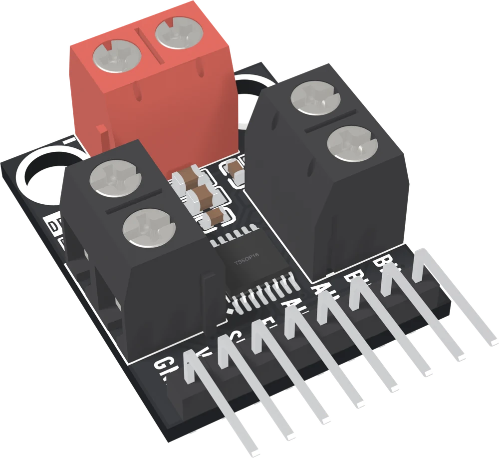
The power input and both motor outputs each have two footprints joined pad to pad, a KF301 screw block and a two-pin 2.54 mm header, so you choose per interface. Fitted, the screw blocks cover the front's pad names; the back's stay readable.
Pinout
| Interface | Pads | What it carries |
|---|---|---|
| Power, top edge | GND (left, −), VM (right, +) | The only supply. 2.7 – 10.8 V |
| Motor A, left edge | AOUT1 (upper), AOUT2 (lower) | Driven by AIN1 and AIN2 |
| Motor B, right edge | BOUT1 (upper), BOUT2 (lower) | Driven by BIN1 and BIN2 |
| Control, bottom edge | 8 pins, below | Logic, plus VM and GND brought out |
The control header runs, from the square pad on the left:
| 1 | 2 | 3 | 4 | 5 | 6 | 7 | 8 |
|---|---|---|---|---|---|---|---|
| GND | VM | SLP | FLT | AIN1 | AIN2 | BIN1 | BIN2 |
The signal pins go straight to the chip, with no resistors, pull-ups or pull-downs on the board.
Wiring, in four lines
- VM and GND to the motor supply, at the power terminal or header pins 1 and 2.
- GND common with your microcontroller's ground.
- SLP to a GPIO you set high, or to VM through 20 – 75 kΩ.
- AIN1, AIN2 (and BIN1, BIN2 for a second motor) to GPIOs; FLT to one with
INPUT_PULLUPif you want faults.
The red LED lights as soon as VM arrives. It says nothing about SLP. Sleep is the default is why an unwired SLP is a definite low, and the four states is where PWM goes, in fast decay or slow.
Where to start
The handbook below is eleven short articles with a working figure in each. If the board is new to you, start with what you are holding. If it is wired and does nothing, sleep is the default. If it runs and then stops, reading the fault pin. The six-step guide is the same board with one connector lit at a time, and the board in 3D turns it over so you can see which holes to wire.
When it doesn’t work
- Nothing happens, and the red LED is on.
- SLP is unwired, and unwired means asleep. The chip has a 500 kΩ pulldown on that pin and this board fits no pull-up, so an unconnected SLP is a definite low. The LED sits across VM and lights whether the chip is asleep or not, so it proves only that the supply arrived. Drive SLP high from a GPIO, or tie it to VM through a 20 to 75 kΩ resistor, never a bare wire.
- SLP is wired but the motor still does not move.
- SLP needs 2.5 V to be sure of reading high, stricter than the 2.0 V of AIN1, AIN2, BIN1 and BIN2. A 3.3 V pin clears it. A signal between 2.0 and 2.5 V, such as the output of a divider, drives the motor inputs and may leave the driver asleep. Allow up to 1 ms after SLP goes high before the outputs respond.
- The fault pin never triggers, even when the motor stalls.
- FLT is open drain with no pull-up fitted, so it floats until you enable INPUT_PULLUP. And the trip is at 2 to 3.3 A: a small motor's stall current is often well below that, and then there is no fault to report. A trip that does happen holds FLT low for 1.35 ms before the driver retries, which a slow polling loop misses. Attach a falling-edge interrupt.
- Both motors turn the same way when they should mirror each other.
- That is wiring, not the board. The upper pad is OUT1 on both motor terminals, so two motors wired the same way behave the same way. Swap the two wires on one motor. With the screw blocks fitted, the back of the board still prints 1 (OUT1) above 2 beside each motor's pads.
- A 5 V stepper runs hot, or the driver does.
- R1 and R2 are 0 Ω, which switches off the chip's current regulation. Coil current at standstill is VM divided by the winding resistance, so a 5 V stepper wants VM at 5 V, not 10.8. The chip is rated for 1.5 A per bridge continuously; the 2 – 3.3 A overcurrent trip is protection, not a rating.