Which pad is OUT1
On both motor terminals the upper pad is OUT1. That single fact decides whether two motors wired identically drive a chassis forward or spin it on the spot, and the board prints it on both faces.
The same pad order on both terminals
With the component side up and the header at the bottom, Motor A is the terminal on the left edge and Motor B the one on the right. On both, the upper pad is OUT1 and the lower pad is OUT2. AIN1 drives AOUT1, BIN1 drives BOUT1.
That consistency is what causes the problem. Wire two motors the same way, red to the upper pad on each, and they receive the same drive and turn the same way, which on opposite sides of a chassis is a spin rather than a drive.
Fix it in copper, not in code
Swap the two leads on one motor. That is the entire fix, and it is the one that stays true when somebody else picks up the project. With screw blocks fitted it is two screws.
The alternative is a negated channel in software, which works and then misleads every later reader of that file. It also breaks the moment the chassis is rewired by someone who assumed the two channels behaved alike.
Reading it with the blocks on
The top's AOUT1 and BOUT1 are under the screw blocks once they are fitted. The back is not.
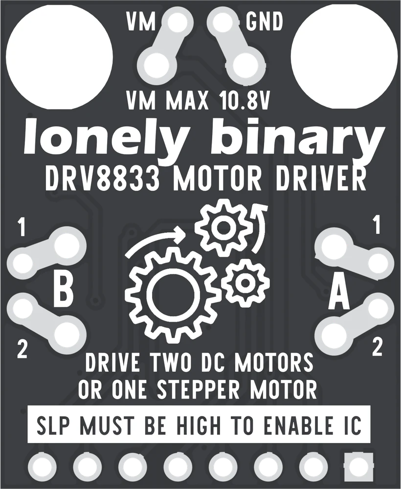
The pads go through the board, so the hole beside a 1 on the back is the hole marked AOUT1 or BOUT1 on the front. Turn the board over whenever you need to check, with the blocks on or off.
When it does not work
That is the expected result of wiring both motors the same way, because both terminals put OUT1 on the upper pad. Swap the two leads on one motor. Nothing is wrong with the board and nothing is wrong with the code.
It is, once. It is a sign flip that whoever reads the code next has to hold in their head on every line that touches channel B, and it stops being true the day somebody rewires the chassis. Swap the wires.
Turn the board over. The back prints 1 above 2 beside each motor's pads, and 1 is OUT1. It is mirrored from the back, so A is on the right, but the 1 and the 2 are beside the same holes the leads go into.
One supply pin, a window with two edges, and a nominal 12 V battery pack that is already outside it before you plug anything in.
The only supply →Edit this page — content/books/drv8833/which-pad-is-out1.mdx
Questions about this product
See what other owners have asked, and read their solutions.
DRV8833 Dual Motor Driver
Loading discussions…
Discuss this article
Ask about this page. The answer stays here, on the page it belongs to, for whoever hits the same wall next.