What you are holding
Two H-bridges in one package, four control pins, two motors. There is no logic supply on this board, and knowing why explains most of the rest of it.
What is on the board
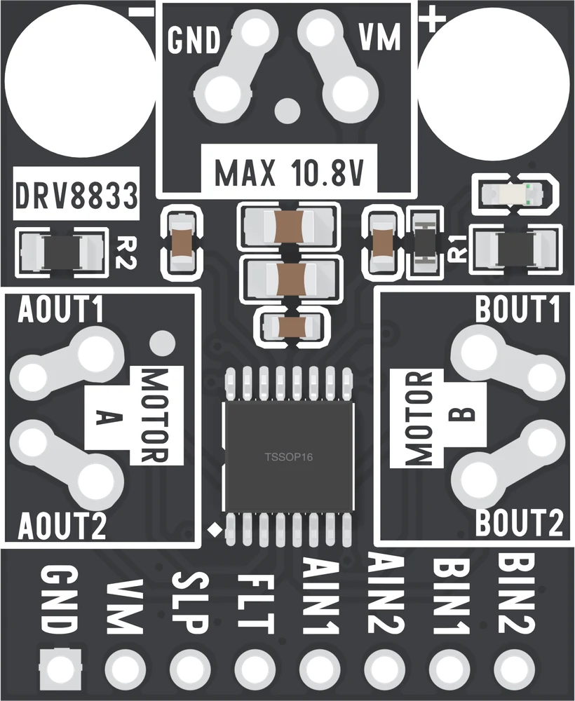
The chip in the middle is a TI DRV8833 in its exposed-pad package. Around it: three capacitors on VM, one for the chip's charge pump, one on its internal supply, R1 and R2, and a red LED with its resistor. Every connector position is empty.
The power terminal takes VM and GND. Each motor terminal has two outputs. The control header has eight pins, and its signal pins go straight to the chip: there are no resistors, pull-ups or pull-downs between them.
Two H-bridges, and what that buys
An H-bridge is four switches in a square with the motor across the middle. Close the top-left and bottom-right pair and current crosses the motor one way; close the other pair and it crosses the other way.
The two stopped states follow from the square. Both inputs low turns all four switches off: the outputs float and the motor freewheels, which is coast. Both inputs high turns on the two low-side switches: the winding is shorted through them, a spinning motor drives current round that loop against itself, and it stops fast, which is brake.
Two bridges sit in one package, each with two inputs, so four GPIO pins give you two DC motors turning either way. Or one bipolar stepper, because a bipolar stepper is two coils with no common connection, which is two bridges' worth of load.
One supply, and no logic rail
VM is the only supply. The chip makes its own internal supply from it, which is why there is no 3.3 V input. The range is 2.7 to 10.8 V; the absolute maximum is 11.8 V. A supply that sags takes the driver's logic down with it, not only its torque. That is its own article.
The LED says VM, and only VM
LED1 is red, and it sits with a 5.1 kΩ resistor straight across VM and ground. It lights whenever VM is present, whether the chip is asleep or awake, faulted or running. A lit LED proves the supply reached the board. It says nothing about SLP, which is the pin that actually decides whether the motors turn.
It also costs current. Worked out rather than measured, it draws about 0.6 mA at 5 V and about 1.7 mA at 10.8 V, all the time, which matters on a battery robot more than the chip's own sleep current does.
What the board leaves to you
R1 and R2 are 0 Ω links from the chip's current-sense pins to ground. That switches off the chip's current regulation: nothing limits motor current except the supply, the winding and the overcurrent trip. For a DC motor that is what you want. For a stepper it is the thing to design around.
And there is no pull-up on the fault pin, so FLT reads as noise until your code turns one on. Both have articles of their own later in this book.
When it does not work
There is nowhere because there is nothing to connect. The DRV8833 makes its own internal supply out of VM, so the board has power in, two motor outputs and a control header, and no logic supply input. A 3.3 V wire from your dev board belongs on none of them.
The LED sits across VM and ground through a resistor, so it proves VM is there and nothing more. It stays lit with the driver asleep. Check SLP next: it has to be high before anything else on the board does anything.
Both channels wake together when SLP goes high. An unwired channel's inputs are pulled low inside the chip, which is the coast state: all four switches off, nothing drawn. Leaving channel B unconnected is fine.
Nothing is soldered to this board when it arrives. The screw blocks and header are in the bag, and which ones go where is your decision.
Why it ships bare →Edit this page — content/books/drv8833/what-you-are-holding.mdx
Questions about this product
See what other owners have asked, and read their solutions.
DRV8833 Dual Motor Driver
Loading discussions…
Discuss this article
Ask about this page. The answer stays here, on the page it belongs to, for whoever hits the same wall next.