The board, end to end
Thirteen components, and the only one that makes a decision is on the face you never look at. Here is the board from the socket to the screw terminal.
The tour
Power comes in at one end and leaves at the other, and everything in between is about deciding how much of it.
The socket is a 16-pin USB-C receptacle, hanging about 0.7 mm over the edge of the board so the plug's shell has somewhere to go. It brings in VBUS, ground, the two data pins and — the ones that matter here — CC1 and CC2, the two configuration pins the negotiation happens on.
The chip is underneath
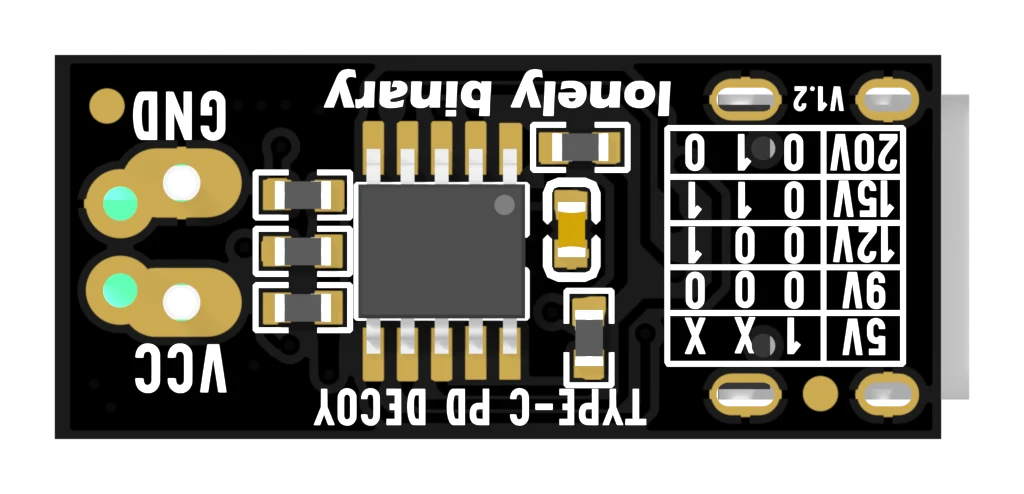
The chip is a CH224K from WCH, in a ten-pin ESSOP package. It is a USB Power Delivery 3.0 sink controller and it does exactly one thing: read three pins, ask the charger for the corresponding voltage, and hold it there. It has no memory, no firmware and nothing to configure beyond those three pins.
Around it are five resistors and a capacitor, and none of them is optional:
- Three 10 kΩ resistors pull the three configuration pins up, because this chip has no pull-ups of its own.
- 1 kΩ feeds the chip's own supply pin from VBUS. It is not a divider — the chip regulates its own 3.3 V internally and the resistor only limits the current, which is why the same 1 kΩ works at 5 V and at 20 V.
- 10 kΩ between VBUS and the chip's voltage-sense pin, because that pin is rated to 13.5 V and this board is asked to reach 20 V.
- 1 µF across the chip's supply, which its datasheet asks for by name.
What the top face gives you
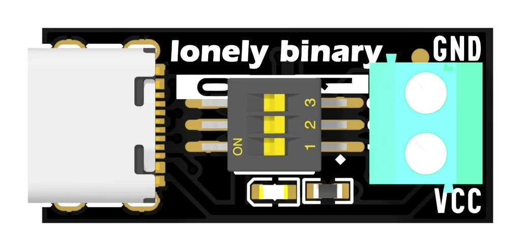
The three levers in the middle are the interface. The red LED below them means the board has power, and — as the next chapter explains at some length — it means nothing else at all. The green block at the right is a two-way screw terminal: GND is the hole nearer the top edge and the GND lettering, VCC is the lower one.
The board is 1.62 mm thick, which is the usual 1.6 mm, so it fits anything that expects a standard PCB.
When it does not work
Turn it over. The CH224K is a ten-pin package on the underside, in the middle, beside five resistors and a capacitor. The top face carries only the socket, the switch, the LED and the terminal, which is why the board looks emptier than it is.
That is the voltage table: five rows, each a voltage and a pattern of three 0s and 1s for the three levers. It is the same table as in the chip's datasheet. The article on the three switches reads it row by row.
The board revision, not a voltage. It says which version of this design you are holding, which matters only if a future revision changes something — the pin order and the switch table on V1.2 are as described throughout this handbook.
A 3.5 mm screw terminal and a 2.54 mm header pair, on the same copper, 1.8 mm apart — and why you can only use one.
Two ways out, one pair of nets →Edit this page — content/books/pd-trigger/the-board-end-to-end.mdx
Questions about this product
See what other owners have asked, and read their solutions.
USB-C PD Trigger, 100 W Decoy 5–20 V, 12-Pack
Loading discussions…
Discuss this article
Ask about this page. The answer stays here, on the page it belongs to, for whoever hits the same wall next.