Both sides of the header
The front of the board is printed with SPI names and two holes marked NC. Turn it over and the same two holes read DATA2 and DATA1. Both faces are correct, and a reader who only ever sees one of them loses two thirds of the speed.
One header, two vocabularies
The front of the board is labelled for SPI, because SPI is what most people wire first: CS, MOSI, SCK, MISO, plus 3V3 and GND, and two holes it has no name for. The back of the board is labelled for the SD bus, where those same holes are DATA3, CMD, CLK, DATA0, DATA2 and DATA1.
| Front | Back | In SPI | In 1-bit | In 4-bit |
|---|---|---|---|---|
| GND | GND | GND | GND | GND |
| 3V3 | 3V3 | 3.3 V | 3.3 V | 3.3 V |
| NC | DATA2 | — | — | D2 |
| CS | DATA3 | CS | — | D3 |
| MOSI | CMD | MOSI | CMD | CMD |
| SCK | CLK | SCK | CLK | CLK |
| MISO | DATA0 | MISO | D0 | D0 |
| NC | DATA1 | — | — | D1 |
| CD | CD | switch | switch | switch |
| WP | WP | switch | switch | switch |
The last two rows are on the full-size board only, and they are switches rather than bus lines — no mode uses them and no mode has to.
The back of the board
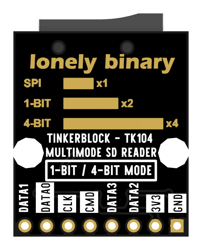
This is not a mistake and it is not two revisions of the board. It is one header labelled for the two things it can be. The bar chart on the back is the argument for turning it over: one data line in SPI, one in SD 1-bit mode, four in SD 4-bit mode.
Wire by position
The safe habit is to count holes from the GND end and ignore every name until the wire is in. GND is pin 1 on both boards, 3V3 is pin 2, and the six signals follow in the same order on both. Then check the names against the mode you are in.
That is also the habit that survives the sketch, whose macros are named after
neither face: SD_MOSI in the SPI example and SDMMC_CMD in the 4-bit example
are both pin 5.
The two you will come back for
The holes printed NC are the whole of the difference between 1.6 MB/s and 5 MB/s. They are wired, they are pulled up, and leaving them empty is a perfectly valid choice — it is what SPI mode is. How fast it goes is what they are worth.
When it does not work
No. They are wired to the card through a 22 Ω resistor and pulled up to 3V3 through 10 kΩ, exactly like the other four signals. NC here means not needed in SPI mode, which is the mode the front of the board is labelled for. Turn the board over: those holes read DATA2 and DATA1.
Because they are the same wire. In SPI mode the host holds that line low to select the card, and in SD mode the card uses it as its fourth data line. One pin, two jobs, decided at power-up by which of them the host does first.
All three are the same hole. The sketch's macro name, the front silkscreen and the back silkscreen are three vocabularies for one wire. Wire by position — the hole — and read the names as a check, not as an instruction.
SPI is not a bus you can cross over. MOSI on your board goes to MOSI on this one, MISO to MISO. There is no crossing anywhere in SPI, unlike a serial port, where TX does go to RX.
One instant at power-up decides which protocol you get, and it does not change afterwards.
SPI mode or SD mode →Edit this page — content/books/sd/reading-the-header.mdx
Questions about this product
See what other owners have asked, and read their solutions.
This page covers several products. Choose yours to see the right discussions.
Discuss this article
Ask about this page. The answer stays here, on the page it belongs to, for whoever hits the same wall next.