
Eight holes, in order
BL, RST, DC, SCL, MOSI, CS, 3V3, GND: the order the back face prints the eight holes, with the backlight first and the supply second from last. The clock is labelled SCL even though this is SPI, and there is no MISO.
The row, in both orders
Every board has the same eight holes at 2.54 mm, and the same eight names. The glass-side face prints them BL RST DC SCL MOSI CS 3V3 GND. The connector face, the one with the sockets and the jumpers, prints the same row mirrored, so it reads GND 3V3 CS MOSI SCL DC RST BL. The net list counts from GND.
Nobody guesses this order. The backlight is at one end and the supply is next to the ground at the other, which is the opposite of how almost every module you will meet is laid out. Read the labels rather than counting from a photograph.
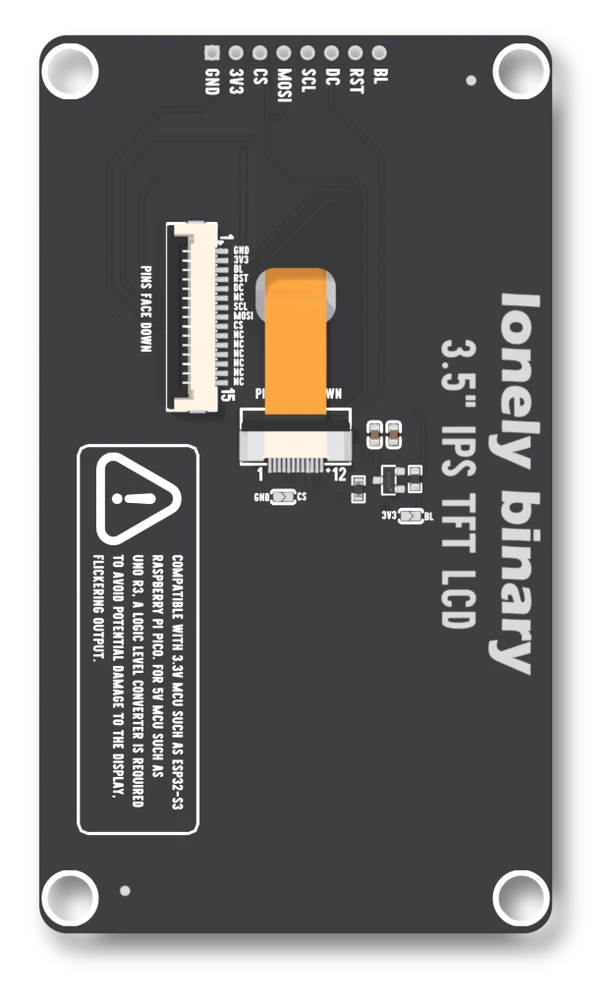
Seven of the eight before anything is drawn
3V3 and GND are the supply. SCL and MOSI carry the picture. DC, RST and CS decide what the picture means: DC says whether the byte on the wire is a command or a pixel, RST gives the controller a clean start, and CS says this display is the one being addressed.
Get any of those seven wrong and nothing is drawn, or something white is, and the failures look alike from across the desk. That is what the fault article is for.
And two names that catch people
The clock hole says SCL. On most boards SCL is an I2C name and the SPI clock is SCK, but the silkscreen here uses SCL and there is no other clock. It is an SPI clock.
There is no MISO. Nothing comes back out of these panels: you write pixels and they hold the picture, and the board has no hole you could read one from. A library that asks for a MISO pin wants to be told there is not one.
BL is the hole that is optional and does not feel it
The backlight is a separate circuit from the picture, and the board holds it off. BL goes to the gate of a transistor with a 10 kΩ resistor on it, so with BL unconnected the controller is drawn on perfectly and the lamp is dark, which looks like a panel that is not working at all.
Drive it from a GPIO and you can dim it, which is different inside on the 0.96 inch than on the other five. Or bridge the BL jumper and forget about it: the two jumpers have an article of their own.
When it does not work
The clock is labelled SCL on these boards. SCL is normally an I2C name and SCK an SPI one, but the silkscreen here uses SCL for the SPI clock and there is no second clock to find. Wire it to your board's SPI clock: GPIO 12 on the library's ESP32-S3 wiring, GPIO 18 on a classic ESP32.
Correct, and it is not missing. The panel is written to and never read from, so the only data line is MOSI. If a library asks for a MISO pin, give it -1 or whatever that library uses for none. The Lonely Binary library never asks.
You can, and the picture will be drawn with the lamp off, which looks exactly like a dead display. The board holds the lamp off until BL is driven. Either drive BL from a GPIO, or bridge the BL solder jumper and leave the hole alone. A floating BL with the jumper open is the one option that wastes an evening.
Yes, or bridge the CS solder jumper, which ties CS to GND. Nothing else on the board holds it low, and a CS that floats is a controller that may or may not listen. One display still needs a pin, or the jumper.
They do, and both are right. The row of holes goes through the board and the silkscreen prints the names on each face so that they read left to right from that face. From the glass side it reads BL first; from the connector side it reads GND first. The net list counts from GND, so GND is hole 1.
Two ways onto the same eight signals, and what the 15-way socket does and does not carry.
The ribbon, or the row of holes →Edit this page — content/books/lcd/eight-pads-in-order.mdx
Questions about this product
See what other owners have asked, and read their solutions.
This page covers several products. Choose yours to see the right discussions.
Discuss this article
Ask about this page. The answer stays here, on the page it belongs to, for whoever hits the same wall next.