
The 2.0 inch board
A 240 × 320 picture on a 36.0 × 64.0 mm board, 30.6 × 40.8 mm of it lit: the smallest pixels in the kit. Its panel socket is 14-way, and its panel's own sheet agrees with it contact for contact, which makes it the easiest of the six to check by eye.
What it is for
240 × 320 pixels is 76,800 of them: 153,600 bytes a frame, which at the library's 40 MHz clock is at least 30.7 ms on the wire. Controller in the library's table: ST7789. The panel's own sheet does not name one.
The lit area is 30.6 × 40.8 mm, which makes the pixel 0.1275 mm: the smallest of the six, about 200 to the inch. It suits a small dashboard where the text should look printed rather than drawn.
Outline and holes
The board is 36.0 mm across and 64.0 mm tall, 1.6 mm thick, with four 4.8 mm holes 24.0 mm apart across and 56.0 mm down, 6.0 mm in from the sides and 4.0 mm from the top and bottom. The header holes are 2.54 mm apart and 17.78 mm across, centred on the top edge, pin 1 (GND) the square one at the left.
The glass module is 34.6 × 47.8 mm on the back; the tail comes through a slot 10.2 mm wide and 6 mm tall.
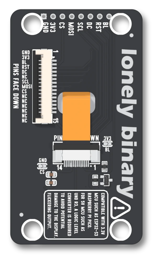
The socket the panel plugs into
The ribbon goes into FPC1, a 14-way, 0.5 mm socket (KH-CL0.5-H2.0-14PIN-SMT). Its pin 1 is at the right-hand end with the header at the top, and the silkscreen numbers it 14 to 1 from the left. What the board wires to each pin:
| Pin | Wired to | |
|---|---|---|
| 1 | not connected | |
| 2 | GND | |
| 3 | the lamp's low side | through R6 and Q2 |
| 4 | 3V3 | |
| 5 | GND | |
| 6 | RST | |
| 7 | DC | |
| 8 | MOSI | |
| 9 | SCL | |
| 10, 11 | 3V3 | |
| 12 | CS | |
| 13 | GND | |
| 14 | not connected |
The panel's own sheet lists the same fourteen in the same order, so this socket and that tail can be read side by side: its pin 4 is the lamp's anode, 10 is the logic supply and 11 the I/O supply, and the board puts all three on 3V3. Three grounds, three 3V3 and a lamp pin leave five signals, and those are the five the header carries.
The backlight
Q2, a BSS138 N-channel transistor, sits on the low side of the lamp: its gate is the BL pad with R2 (10 kΩ) from gate to GND, its drain goes through R6 (2.2 Ω) to socket pin 3, and the lamp's high side is on 3V3. BL HIGH is lit; a BL pad nothing drives is dark.
Its two jumpers
Both are open as shipped.
CS, silkscreen GND CS, at the left, level with the socket: bridged, CS is tied to GND and the display is always selected. Do not then drive the CS pad.SB3, silkscreen 3V3 BL, at the right, above the socket: bridged, BL is tied to 3V3 and the lamp is lit whenever there is power. Leave the BL pad unconnected.
Both are covered in the two solder jumpers.
Wiring and the constant
// 3V3 -> 3V3        GND -> GND
// SCL -> GPIO 12    MOSI -> GPIO 11      (classic ESP32: 18, 23)
// DC  -> GPIO 2     RST  -> GPIO 42      (classic ESP32: 2, 4)
// CS  -> GPIO 10    BL   -> GPIO 41      (classic ESP32: 15, 32)
LB_Display display(LB_TFT_20);#include <LonelyBinaryDisplay.h>
LB_Display display(LB_TFT_20); // the only line that changes per panelfrom lb_display import LBDisplay
from lb_panels import TFT_20 # the only line that changes per panel
d = LBDisplay(TFT_20)3.3 V only. Wiring for your board has the pins for other chips.
What is different about this one
Not much, and that is the point. The 2.0, 2.4 and 2.8 inch are one 240 × 320 picture on three sizes of glass; this is the smallest of the three, so it is the sharpest, and a sketch moves between them by one constant.
On the board itself, the things to know are the 14 contacts (the most of the six), the two unused ones at the ends, and that its header row is holes in the model, with no pins drawn. Next, first light runs the self-test.
When it does not work
Unchanged, with one token different. The 2.0, 2.4 and 2.8 share a controller and a 240 × 320 resolution, and the pins belong to the breakout, so LB_TFT_24 becomes LB_TFT_20 and nothing else in the sketch moves. The layout is the same in pixels and smaller on the glass.
The same pixel count on less glass: 0.1275 mm a pixel against 0.153 on the 2.4, so a 16-pixel line of text is 2.0 mm tall instead of 2.4. Nothing is wrong. Raise the text size by one step, or accept the denser picture, which is what this size is for.
The bill of materials for this board lists no header, and its 3D model shows eight plated holes and nothing in them. Solder an 8-pin 2.54 mm strip, or use the 15-way ribbon socket and skip the holes. Which of those your box makes easiest I cannot tell from the files.
That is BL. R2 holds Q2's gate low, so the lamp is off until BL is driven HIGH, and a BL wire that goes nowhere leaves it off. Drive BL from a pin, or bridge the 3V3 BL jumper to light it for good and then leave the BL pad alone.
The same picture on bigger glass, with a 1.0 mm panel socket.
The 2.4 inch board →Edit this page — content/books/lcd/the-2-0-inch-board.mdx
Questions about this product
See what other owners have asked, and read their solutions.
This page covers several products. Choose yours to see the right discussions.
Discuss this article
Ask about this page. The answer stays here, on the page it belongs to, for whoever hits the same wall next.