
The 2.8 inch board
The same 240 × 320 picture as the 2.0 and 2.4, spread over 43.2 × 57.6 mm of glass on a 48.6 × 79.8 mm board. It is the only one of the six that prints a revision, V1.1, and its panel socket counts from the left where the three before it count from the right.
What it is for
240 × 320 pixels is 76,800 of them: 153,600 bytes a frame, which at the library's 40 MHz clock is at least 30.7 ms on the wire. Controller in the library's table: ST7789. The lit area is 43.2 × 57.6 mm, 0.18 mm a pixel.
It is the same picture as the 2.4 inch, spread wider, so it reads from further away and shows no more.
Outline and holes
The board is 48.6 mm across and 79.8 mm tall, 1.6 mm thick, with four 4.8 mm holes 40.0 mm apart across and 72.0 mm down, 4.3 mm in from the sides. The header holes are 2.54 mm apart, 17.78 mm across, pin 1 (GND) at the left.
The glass module is 47.2 × 66.2 mm on the back; the tail comes through a slot 8.5 mm wide and 6 mm tall.
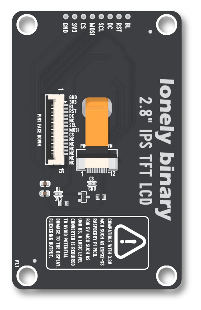
The socket the panel plugs into
The ribbon goes into FPC1, a 12-way, 0.5 mm socket (KH-CL0.5-H2.0-12PIN-SMT). Its pin 1 is at the left end with the header at the top, and the silkscreen numbers it 1 to 12 left to right. What the board wires to each pin:
| Pin | Wired to | |
|---|---|---|
| 1 | GND | |
| 2 | the lamp's low side | through R1 and Q1 |
| 3, 4 | 3V3 | |
| 5 | GND | |
| 6 | not connected | |
| 7 | DC | |
| 8 | CS | |
| 9 | SCL | |
| 10 | MOSI | |
| 11 | RST | |
| 12 | GND |
That is what the board does with each contact. The panel's sheet numbers its twelve contacts differently from this socket, so this page does not print it and does not rely on it; match the tail to the socket by looking at them.
The backlight
Q1, a BSS138 N-channel transistor, sits on the low side of the lamp: its gate is the BL pad with R2 (10 kΩ) from gate to GND, its drain goes through R1 (2.2 Ω) to socket pin 2, and the lamp's high side is on 3V3. BL HIGH is lit; a BL pad nothing drives is dark.
Its two jumpers
Both are open as shipped.
CS, silkscreen CS GND, just below the socket: bridged, CS is tied to GND and the display is always selected. Do not then drive the CS pad.3V3, silkscreen BL 3V3, at the lower left: bridged, BL is tied to 3V3 and the lamp is lit whenever there is power. Leave the BL pad unconnected.
Both are covered in the two solder jumpers.
Wiring and the constant
// 3V3 -> 3V3        GND -> GND
// SCL -> GPIO 12    MOSI -> GPIO 11      (classic ESP32: 18, 23)
// DC  -> GPIO 2     RST  -> GPIO 42      (classic ESP32: 2, 4)
// CS  -> GPIO 10    BL   -> GPIO 41      (classic ESP32: 15, 32)
LB_Display display(LB_TFT_28);#include <LonelyBinaryDisplay.h>
LB_Display display(LB_TFT_28); // the only line that changes per panelfrom lb_display import LBDisplay
from lb_panels import TFT_28 # the only line that changes per panel
d = LBDisplay(TFT_28)3.3 V only. Wiring for your board has the pins for other chips.
What is different about this one
Two things about the board, neither about the picture. It prints V1.1 on its front silkscreen, which no other board of the six does, and it counts its panel socket from the left.
Its sibling in the table is the 3.5 inch: the same socket part, the same numbering direction, and nearly the same wiring, differing only in pin 5, which is GND here and not connected on the 3.5. Next, first light runs the self-test.
When it does not work
This is the only board of the six that prints one; the other five print none, so a missing revision on them means nothing. The 3D and drawing files for this board are released under the tag lcd280-v1.1 in the cad repository, which is the revision as printed.
No. The vendor's drawing carries a stray capacitive-touch note, but the socket on the board has no touch pins, there is no touch controller on the board, and the library lists no touch for this panel. The glass is display only.
This socket's pin 1 is at the left with the header at the top; the 1.8, 2.0 and 2.4 boards number theirs from the right. Read the printed numbers on the board, not a position, and do not carry a pin number between boards.
Same 240 × 320 on bigger glass: 0.18 mm a pixel against 0.1275 on the 2.0. For a sharper picture of the same program, move down to the 2.0 or 2.4 with one constant.
Edit this page — content/books/lcd/the-2-8-inch-board.mdx
Questions about this product
See what other owners have asked, and read their solutions.
This page covers several products. Choose yours to see the right discussions.
Discuss this article
Ask about this page. The answer stays here, on the page it belongs to, for whoever hits the same wall next.