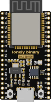
 InteractiveOpen the ESP32 in 3DTurn the real board over and click any of its 38 holes. Every pad is placed from this design’s own net list.Open in 3D →
Reading this board
Two 19-pin headers, 38 holes: 26 GPIO, six power, and six pads in no net at all. The rows are 25.4 mm apart on a 2.54 mm pitch — ten breadboard columns, so a build has one spare column either side of the board. The module is an ESP32-WROOM-32E, with 4, 8 or 16 MB of flash depending on the variant and no PSRAM on any of them.
Every pin below is read from this design's own net list, so the hole in the table is the hole on your desk. Open the board in 3D to turn it over and click one.
Fifteen of the 26 GPIO have nothing attached and nothing sampled at reset. Six more can be trusted with an analog input on a connected board. The rest are the next two sections.
The six pads that go nowhere
The holes silkscreened 6, 7, 8, 9, 10 and 11 are in no net. On almost every other classic-ESP32 board those six positions carry the module's flash bus, and driving one stops the chip dead. Here they are drilled, plated and labelled for pin-compatibility and then routed nowhere — so unlike most boards, you cannot crash this one by touching them. You also cannot use them. There is no copper on the other side of the pad.
Note what that does not mean. The flash inside the module still runs on the
chip's GPIO6 to GPIO11; those lines simply never reach a header. Software that
addresses those GPIO numbers is still talking to the flash bus, and still
crashes — Serial1 on its default pins is the one people hit, because the
Arduino core puts it on GPIO9 and GPIO10.
When it will not boot
GPIO0, 2, 5, 12 and 15 are sampled as the chip leaves reset, to pick boot mode, flash voltage and SDIO timing. Afterwards they are yours — but a board that flashes over USB and then will not start on its own supply is almost always one of those five. GPIO12 is the usual culprit: pulled high it selects the wrong flash voltage and the chip never gets as far as your code. Boot it bare, then add one wire at a time.
Three of the five — GPIO0, 5 and 15 — also emit a PWM burst while the chip
starts. An LED on one flickers at power-up, and a servo or a MOSFET gate sees a
few milliseconds of noise before setup() runs.
The RGB LED on GPIO2 is a worked example of getting this right by accident. It is a WS2812, and a WS2812 data line idles low — which is the level the strap wants, so the LED being there costs nothing. Wire something to GPIO2 that idles high and flashing stops working.
Input only, and it is not the ADC that suffers
GPIO34, 35, 36 and 39 have no output driver, no PWM, and no internal pull-up or
pull-down. The last one is what bites: a button on one of these needs a real
resistor, because INPUT_PULLUP has nothing to switch on.
They are also the best analog inputs the board has — see below — and that is not a coincidence worth working around. Reading a voltage never needed an output driver.
Power
5V is USB bus voltage, and it arrives through a Schottky diode. That matters
in both directions: you can feed the board from this pin without pushing
current back out into a plugged-in computer, and the pin sits a little below
what the cable actually delivers.
3V3 is the output of an AMS1117-3.3, and the module, the bridge and both LEDs
already draw from it. Budget about 500 mA for your own parts, less once the
radio is transmitting — the regulator is the ceiling, not what the USB cable
could deliver.
EN is the chip-enable line, pulled up, with a capacitor that holds the chip
in reset for a moment after power arrives so it does not start running while
the 3.3 V rail is still on its way up. Tie it to ground through a button and
you have a second reset button; the one on the board does exactly that.
All three GND holes are the same net.
Buses
Nothing is fixed on this chip, but these are the defaults the Arduino core assumes and the ones the examples on this site use:
| Bus | Pins | Note |
|---|---|---|
| I²C | SDA GPIO21, SCL GPIO22 | Remappable; 4.7 kΩ pull-ups needed if the module has none |
| SPI (VSPI) | MOSI GPIO23, MISO GPIO19, SCK GPIO18, SS GPIO5 | SS lands on a strapping pin — see below |
| UART0 | TX GPIO1, RX GPIO3 | The USB serial console — leave it alone |
| UART2 | TX GPIO17, RX GPIO16 | Serial2, and yours |
Serial1 is missing from that table on purpose. Its default pins are the flash
bus, as above; use Serial2, or pass your own pins to Serial1.begin().
The chip-select landing on GPIO5 is the one worth designing around. A
chip-select that twitches while the chip boots can make an SPI peripheral see a
transaction nobody sent. If a display or an SD card is unreliable only on the
first power-up after the supply comes on, move SS to an ordinary pin and set
it high yourself before the first transfer.
ADC and DAC
The classic ESP32 has two ADCs and they are not interchangeable.
ADC1 works whatever the radio is doing. Eight channels on the die, six of them on this header: GPIO32, 33, 34, 35, 36 and 39. The other two are GPIO37 and GPIO38, which the WROOM module does not bring out at all.
ADC2 stops working the moment Wi-Fi starts. The driver hands the block to
the radio front end, and from then on a read returns an error rather than a
wrong number. That is GPIO0, 2, 4, 12, 13, 14, 15, 25, 26 and 27 — ten pins,
every one of them still fine as digital I/O. An analog reading that goes dead
exactly when you call WiFi.begin() is this, and the fix is to move the input
to an ADC1 pin.
So the analog inputs you can trust on a connected board are the six ADC1 pins, and four of the six are the input-only pins from earlier. That is less awkward than it sounds: reading a voltage never needed an output driver.
GPIO25 and GPIO26 are real analog outputs — DAC1 and DAC2, eight bits each. This is the one thing the classic chip does that the S3 dropped completely: an actual voltage, not a filtered PWM. Both are ADC2 channels as well, which is a limit on reading them, not on driving them.
Capacitive touch is T0 to T9, on GPIO0, 2, 4, 12, 13, 14, 15, 27, 32 and 33.
Pins to leave alone
- GPIO36 — Input only. No output driver, no PWM and no internal pull-up or pull-down, so a button on this pin needs a resistor of its own.
- GPIO39 — Input only. No output driver, no PWM and no internal pull-up or pull-down, so a button on this pin needs a resistor of its own.
- GPIO34 — Input only. No output driver, no PWM and no internal pull-up or pull-down, so a button on this pin needs a resistor of its own.
- GPIO35 — Input only. No output driver, no PWM and no internal pull-up or pull-down, so a button on this pin needs a resistor of its own.
- GPIO25 — ADC2, so analogRead stops working the moment Wi-Fi starts. Unaffected as a digital pin.
- GPIO26 — ADC2, so analogRead stops working the moment Wi-Fi starts. Unaffected as a digital pin.
- GPIO27 — ADC2, so analogRead stops working the moment Wi-Fi starts. Unaffected as a digital pin.
- GPIO14 — ADC2, so analogRead stops working the moment Wi-Fi starts. Unaffected as a digital pin.
- GPIO12 — Strapping pin. Sets the flash voltage. Boot fails if it is pulled high.
- GPIO13 — ADC2, so analogRead stops working the moment Wi-Fi starts. Unaffected as a digital pin.
- 9 — L16. Where a devkit would put the flash bus SHD / SD2. This board routes it nowhere — the net list has no net for this pad.
- 10 — L17. Where a devkit would put the flash bus SWP / SD3. This board routes it nowhere — the net list has no net for this pad.
- 11 — L18. Where a devkit would put the flash bus CSC / CMD. This board routes it nowhere — the net list has no net for this pad.
- GPIO1 — UART0 TX, wired to the USB-UART bridge behind the USB-C port. The chip also prints its boot log here.
- GPIO3 — UART0 RX, wired to the USB-UART bridge behind the USB-C port.
- GPIO5 — Strapping pin. Sets the SDIO timing. Outputs a PWM signal at boot.
- GPIO4 — ADC2, so analogRead stops working the moment Wi-Fi starts. Unaffected as a digital pin.
- GPIO0 — BOOT button, with a 10 kΩ pull-up. Held low at reset it drops the chip into the ROM bootloader.
- GPIO2 — WS2812B RGB LED, single-wire at 800 kHz. The silkscreen says RGB IO2. Note that GPIO2 is also a strapping pin, so whatever you drive on it must be low or floating while the chip comes out of reset — a WS2812 data line idles low, which is why it works here.
- GPIO15 — Strapping pin. Silences the boot log when pulled low. Outputs a PWM signal at boot.
- 8 — R17. Where a devkit would put the flash bus SDI / SD1. This board routes it nowhere — the net list has no net for this pad.
- 7 — R18. Where a devkit would put the flash bus SDO / SD0. This board routes it nowhere — the net list has no net for this pad.
- 6 — R19. Where a devkit would put the flash bus SCK / CLK. This board routes it nowhere — the net list has no net for this pad.
Every pin
| Pin | Name | Functions | Notes |
|---|---|---|---|
| 3V | 3.3 V rail | power | L1. Output of the on-board regulator, not an input. Everything on the board runs from it. Budget what the regulator can spare, not what USB can deliver. |
| EN | EN / reset | power | L2. The regulator enable line, pulled up. Tie it to ground through a button and you have a reset button. |
| GPIO36 | GPIO36 | gpio, adc1, input-only | Input only. No output driver, no PWM and no internal pull-up or pull-down, so a button on this pin needs a resistor of its own. |
| GPIO39 | GPIO39 | gpio, adc1, input-only | Input only. No output driver, no PWM and no internal pull-up or pull-down, so a button on this pin needs a resistor of its own. |
| GPIO34 | GPIO34 | gpio, adc1, input-only | Input only. No output driver, no PWM and no internal pull-up or pull-down, so a button on this pin needs a resistor of its own. |
| GPIO35 | GPIO35 | gpio, adc1, input-only | Input only. No output driver, no PWM and no internal pull-up or pull-down, so a button on this pin needs a resistor of its own. |
| GPIO32 | GPIO32 | gpio, adc1, touch | L7 |
| GPIO33 | GPIO33 | gpio, adc1, touch | L8 |
| GPIO25 | GPIO25 | gpio, adc2, dac | ADC2, so analogRead stops working the moment Wi-Fi starts. Unaffected as a digital pin. |
| GPIO26 | GPIO26 | gpio, adc2, dac | ADC2, so analogRead stops working the moment Wi-Fi starts. Unaffected as a digital pin. |
| GPIO27 | GPIO27 | gpio, adc2, touch | ADC2, so analogRead stops working the moment Wi-Fi starts. Unaffected as a digital pin. |
| GPIO14 | GPIO14 | gpio, adc2, touch | ADC2, so analogRead stops working the moment Wi-Fi starts. Unaffected as a digital pin. |
| GPIO12 | GPIO12 | gpio, adc2, touch | Strapping pin. Sets the flash voltage. Boot fails if it is pulled high. |
| GND | Ground | power | L14. Ground. Several holes so a breadboard build has one nearby wherever it needs it. |
| GPIO13 | GPIO13 | gpio, adc2, touch | ADC2, so analogRead stops working the moment Wi-Fi starts. Unaffected as a digital pin. |
| 9 | Not connected | — | L16. Where a devkit would put the flash bus SHD / SD2. This board routes it nowhere — the net list has no net for this pad. |
| 10 | Not connected | — | L17. Where a devkit would put the flash bus SWP / SD3. This board routes it nowhere — the net list has no net for this pad. |
| 11 | Not connected | — | L18. Where a devkit would put the flash bus CSC / CMD. This board routes it nowhere — the net list has no net for this pad. |
| 5V | 5 V rail | power | L19. The USB rail, upstream of the regulator. Feed the board here if you are not using USB, or take 5 V out if you are. |
| GND | Ground | power | R1. Ground. Several holes so a breadboard build has one nearby wherever it needs it. |
| GPIO23 | GPIO23 | gpio, spi | R2. Arduino default: SPI (VSPI) MOSI. |
| GPIO22 | GPIO22 | gpio, i2c | R3. Arduino default: Wire (I²C) SCL. |
| GPIO1 | TX | gpio, uart | UART0 TX, wired to the USB-UART bridge behind the USB-C port. The chip also prints its boot log here. |
| GPIO3 | RX | gpio, uart | UART0 RX, wired to the USB-UART bridge behind the USB-C port. |
| GPIO21 | GPIO21 | gpio, i2c | R6. Arduino default: Wire (I²C) SDA. |
| GND | Ground | power | R7. Ground. Several holes so a breadboard build has one nearby wherever it needs it. |
| GPIO19 | GPIO19 | gpio, spi | R8. Arduino default: SPI (VSPI) MISO. |
| GPIO18 | GPIO18 | gpio, spi | R9. Arduino default: SPI (VSPI) SCK. |
| GPIO5 | GPIO5 | gpio, spi | Strapping pin. Sets the SDIO timing. Outputs a PWM signal at boot. |
| GPIO17 | GPIO17 | gpio, uart | R11. Arduino default: Serial2 TX. |
| GPIO16 | GPIO16 | gpio, uart | R12. Arduino default: Serial2 RX. |
| GPIO4 | GPIO4 | gpio, adc2, touch | ADC2, so analogRead stops working the moment Wi-Fi starts. Unaffected as a digital pin. |
| GPIO0 | GPIO0 | gpio, adc2, touch | BOOT button, with a 10 kΩ pull-up. Held low at reset it drops the chip into the ROM bootloader. |
| GPIO2 | GPIO2 | gpio, adc2, touch | WS2812B RGB LED, single-wire at 800 kHz. The silkscreen says RGB IO2. Note that GPIO2 is also a strapping pin, so whatever you drive on it must be low or floating while the chip comes out of reset — a WS2812 data line idles low, which is why it works here. |
| GPIO15 | GPIO15 | gpio, adc2, touch | Strapping pin. Silences the boot log when pulled low. Outputs a PWM signal at boot. |
| 8 | Not connected | — | R17. Where a devkit would put the flash bus SDI / SD1. This board routes it nowhere — the net list has no net for this pad. |
| 7 | Not connected | — | R18. Where a devkit would put the flash bus SDO / SD0. This board routes it nowhere — the net list has no net for this pad. |
| 6 | Not connected | — | R19. Where a devkit would put the flash bus SCK / CLK. This board routes it nowhere — the net list has no net for this pad. |
Edit this page — content/pinouts/esp32.mdx