
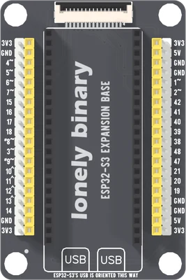
 InteractiveOpen the S3 Expansion in 3DTurn the real board over and click any of its 40 holes. Every pad is placed from this design’s own net list.Open in 3D →
Reading this board
The base has no chip and nothing active on it. An ESP32-S3 Gold Edition plugs into the two sockets down the middle, antenna end toward the display connector, and the base brings most of its pins out along both edges. Each edge has two 20-way strips side by side on the same nets, hole for hole, so there are 80 holes in 40 positions: 28 GPIOs, plus 3V3, 5V and GND repeated along the way.
The order is the S3 Gold's own, read from this design's net list, so anything that is true of a pin on the S3 Gold pinout is true of the same pin here. Open the base in 3D and click either strip; the handbook covers using it.
What the edge carries
| Edge | Top to bottom, display end first |
|---|---|
| Left | 3V3, GND, 4, 5, 6, 7, 15, 16, 17, 18, 8, 3, 9, 10, 11, 12, 13, 14, GND, 3V3 |
| Right | 3V3, 5V, GND, GND, 1, 2, 42, 41, 40, 39, 38, 48, 47, 21, 20, 19, GND, GND, 5V, 3V3 |
That is 16 GPIOs on the left and 12 on the right. 5V is on the right strips only, at the second and second-last holes; the left has none.
The eight that stay on the sockets
A strip is 20 holes and a socket is 22, and the dev board has 36 GPIOs, so some do not come out. These eight go to the sockets and no further: GPIO0, 35, 36, 37, 43, 44, 45 and 46. RST stays on the socket as well.
| GPIO | Why you would not have wanted it |
|---|---|
| 35, 36, 37 | Octal PSRAM on the N16R8 module the kit ships. Driving one crashes the board. |
| 43, 44 | The serial link to the USB-serial chip. |
| 0, 45, 46 | Strapping pins, read at reset to decide how the chip boots. |
Everything else on the dev board's edge is on a strip. GPIO19 and 20 are the native USB lines and GPIO3 is a strapping pin that floats by default; they are there if you want them, with those facts attached.
The marks and the back
The top silkscreen prints ~, # and ^ beside some numbers. The back
repeats them as boxes: ADC1 over 3 to 10, I2S over SCL 9 and SDA 8, UART TX
43 and RX 44, SPI MOSI 11, MISO 13, SCK 12, SS 10, and USB D− 19, D+ 20. The
I2S box means I²C; nothing on this board touches I²S. 43 and 44 are on the
back's UART box but are not brought out to a strip.
The display connector
A 15-way FPC socket on a 1.0 mm pitch at the top of the board. Nothing switches its lines: all thirteen signals are the same nets as holes on the strips, so a fitted display owns those GPIOs.
| Contact | Signal | Contact | Signal |
|---|---|---|---|
| 1 | GND | 9 | GPIO10 |
| 2 | 3V3 | 10 | GPIO1 |
| 3 | GPIO41 | 11 | GPIO15 |
| 4 | GPIO42 | 12 | GPIO7 |
| 5 | GPIO2 | 13 | GPIO4 |
| 6 | GPIO13 | 14 | GPIO6 |
| 7 | GPIO12 | 15 | GPIO5 |
| 8 | GPIO11 |
The net list names those lines BL, DC and CS for GPIO41, GPIO2 and GPIO10, and
D2 to D7 for GPIO1, 15, 7, 4, 6 and 5. The back of the board prints contacts
10 and 11 as 20-1 and 22-15; there is no contact 20 or 22 on a 15-way
connector, so that is a typo in the legend and the wiring above is right.
Power
3V3 and 5V are the S3 Gold's own pins passed straight through; the base has
no regulator. 3V3 comes from the S3 Gold's AMS1117 and there is a 3V3 hole at
both ends of every strip. 5V is the dev board's 5V pin, which on USB power is
the cable's 5 V less a diode drop. All the GND holes are the same net.
Pins to leave alone
- GPIO15 — ADC2, so analogRead stops working the moment Wi-Fi starts. Unaffected as a digital pin.
- GPIO16 — ADC2, so analogRead stops working the moment Wi-Fi starts. Unaffected as a digital pin.
- GPIO17 — ADC2, so analogRead stops working the moment Wi-Fi starts. Unaffected as a digital pin.
- GPIO18 — ADC2, so analogRead stops working the moment Wi-Fi starts. Unaffected as a digital pin.
- GPIO3 — Strapping pin. Selects the JTAG source. Floating at reset is the normal state.
- GPIO11 — ADC2, so analogRead stops working the moment Wi-Fi starts. Unaffected as a digital pin.
- GPIO12 — ADC2, so analogRead stops working the moment Wi-Fi starts. Unaffected as a digital pin.
- GPIO13 — ADC2, so analogRead stops working the moment Wi-Fi starts. Unaffected as a digital pin.
- GPIO14 — ADC2, so analogRead stops working the moment Wi-Fi starts. Unaffected as a digital pin.
- GPIO48 — WS2812B RGB LED, single-wire at 800 kHz. The silkscreen says RGB@IO48.
- GPIO20 — Native USB-C, D+ . Wired straight to the USB-Serial-JTAG peripheral, no bridge chip in the path.
- GPIO19 — Native USB-C, D− . Wired straight to the USB-Serial-JTAG peripheral, no bridge chip in the path.
Every pin
| Pin | Name | Functions | Notes |
|---|---|---|---|
| 3V3 | 3.3 V rail | power | L1. Output of the on-board regulator. Everything on the board runs from it, so budget what the regulator can spare, not what USB can deliver. A steady 3.3 V supply can also power the board through it, but never with USB plugged in at the same time. |
| GND | Ground | power | L2. Ground. Several holes so a breadboard build has one nearby wherever it needs it. |
| GPIO4 | GPIO4 | gpio, adc1, touch | L3 |
| GPIO5 | GPIO5 | gpio, adc1, touch | L4 |
| GPIO6 | GPIO6 | gpio, adc1, touch | L5 |
| GPIO7 | GPIO7 | gpio, adc1, touch | L6 |
| GPIO15 | GPIO15 | gpio, adc2 | ADC2, so analogRead stops working the moment Wi-Fi starts. Unaffected as a digital pin. |
| GPIO16 | GPIO16 | gpio, adc2 | ADC2, so analogRead stops working the moment Wi-Fi starts. Unaffected as a digital pin. |
| GPIO17 | GPIO17 | gpio, adc2, uart | ADC2, so analogRead stops working the moment Wi-Fi starts. Unaffected as a digital pin. |
| GPIO18 | GPIO18 | gpio, adc2, uart | ADC2, so analogRead stops working the moment Wi-Fi starts. Unaffected as a digital pin. |
| GPIO8 | GPIO8 | gpio, adc1, touch, i2c | L11. Arduino default: Wire (I²C) SDA. |
| GPIO3 | GPIO3 | gpio, adc1, touch | Strapping pin. Selects the JTAG source. Floating at reset is the normal state. |
| GPIO9 | GPIO9 | gpio, adc1, touch, i2c | L13. Arduino default: Wire (I²C) SCL. |
| GPIO10 | GPIO10 | gpio, adc1, touch, spi | L14. Arduino default: SPI (HSPI) SS. |
| GPIO11 | GPIO11 | gpio, adc2, touch, spi | ADC2, so analogRead stops working the moment Wi-Fi starts. Unaffected as a digital pin. |
| GPIO12 | GPIO12 | gpio, adc2, touch, spi | ADC2, so analogRead stops working the moment Wi-Fi starts. Unaffected as a digital pin. |
| GPIO13 | GPIO13 | gpio, adc2, touch, spi | ADC2, so analogRead stops working the moment Wi-Fi starts. Unaffected as a digital pin. |
| GPIO14 | GPIO14 | gpio, adc2, touch | ADC2, so analogRead stops working the moment Wi-Fi starts. Unaffected as a digital pin. |
| GND | Ground | power | L19. Ground. Several holes so a breadboard build has one nearby wherever it needs it. |
| 3V3 | 3.3 V rail | power | L20. Output of the on-board regulator. Everything on the board runs from it, so budget what the regulator can spare, not what USB can deliver. A steady 3.3 V supply can also power the board through it, but never with USB plugged in at the same time. |
| 3V3 | 3.3 V rail | power | R1. Output of the on-board regulator. Everything on the board runs from it, so budget what the regulator can spare, not what USB can deliver. A steady 3.3 V supply can also power the board through it, but never with USB plugged in at the same time. |
| 5V | 5 V rail | power | R2. The USB rail, upstream of the regulator. Feed the board here if you are not using USB, or take 5 V out if you are. |
| GND | Ground | power | R3. Ground. Several holes so a breadboard build has one nearby wherever it needs it. |
| GND | Ground | power | R4. Ground. Several holes so a breadboard build has one nearby wherever it needs it. |
| GPIO1 | GPIO1 | gpio, adc1, touch | R5 |
| GPIO2 | GPIO2 | gpio, adc1, touch | R6 |
| GPIO42 | GPIO42 | gpio, jtag | R7 |
| GPIO41 | GPIO41 | gpio, jtag | R8 |
| GPIO40 | GPIO40 | gpio, jtag | R9 |
| GPIO39 | GPIO39 | gpio, jtag | R10 |
| GPIO38 | GPIO38 | gpio | R11 |
| GPIO48 | GPIO48 | gpio | WS2812B RGB LED, single-wire at 800 kHz. The silkscreen says RGB@IO48. |
| GPIO47 | GPIO47 | gpio | R13 |
| GPIO21 | GPIO21 | gpio | R14 |
| GPIO20 | GPIO20 | gpio, adc2, usb | Native USB-C, D+ . Wired straight to the USB-Serial-JTAG peripheral, no bridge chip in the path. |
| GPIO19 | GPIO19 | gpio, adc2, usb | Native USB-C, D− . Wired straight to the USB-Serial-JTAG peripheral, no bridge chip in the path. |
| GND | Ground | power | R17. Ground. Several holes so a breadboard build has one nearby wherever it needs it. |
| GND | Ground | power | R18. Ground. Several holes so a breadboard build has one nearby wherever it needs it. |
| 5V | 5 V rail | power | R19. The USB rail, upstream of the regulator. Feed the board here if you are not using USB, or take 5 V out if you are. |
| 3V3 | 3.3 V rail | power | R20. Output of the on-board regulator. Everything on the board runs from it, so budget what the regulator can spare, not what USB can deliver. A steady 3.3 V supply can also power the board through it, but never with USB plugged in at the same time. |
Edit this page — content/pinouts/s3base.mdx