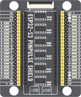
 InteractiveOpen the S3 PinPulse in 3DTurn the real board over and click any of its 44 holes. Every pad is placed from this design’s own net list.Open in 3D →
Reading this board
The shield has no chip of its own. An ESP32-S3 Gold Edition plugs into the socket down the middle, antenna end toward the display connector, and the shield brings each of its 44 header pins out twice: once on a male pin at the outer edge, once on the yellow female socket beside it. The two rows on each side are the same nets, hole for hole, so there are 88 holes and 44 pins: 36 GPIO and eight power.
The order is the S3 Gold's own, read from this design's net list, so anything
that is true of a pin on the S3 Gold pinout is true of the
same pin here. The one difference in print is that this silkscreen labels the
serial pins 43 and 44 rather than TX and RX. Open the shield in
3D and click either row; the handbook
covers using it.
The LEDs
Every GPIO has an LED, lit while the pin is high. The pin does not drive it. Each GPIO goes to one input of a 74HC04 inverter (six chips, 36 gates), the gate output sinks the LED, and the LED's anode goes to 3.3 V through 5.1 kΩ. A high pin pulls the gate output low and the LED lights.
What that costs the pin is one CMOS input: at most 1 µA of leakage and 10 pF. A sensor, a bus or a PWM output does not notice it, and the LED current comes off the 3.3 V rail through the inverter rather than out of the GPIO. Any visible LED drops at least 1.5 V, which leaves under 0.4 mA each, so all 36 lit draw less than 15 mA.
The cost shows up the other way round. A pin nothing is driving flickers.
An inverter input left floating picks up whatever is nearby, so a GPIO your
sketch never set lights and dims when a hand comes close. The back of the board
says as much. Set the pin as an output, or give it INPUT_PULLUP, and it
stops. A pin toggling faster than the eye can follow shows as a glow, not a
blink.
The marks beside the numbers
| Mark | Pins | Meaning |
|---|---|---|
~ | GPIO1 to 10 | ADC1, which keeps working with Wi-Fi on |
# | GPIO8, 9 | I²C defaults: SDA 8, SCL 9 |
^ | GPIO10 to 13 | SPI defaults: SS 10, MOSI 11, SCK 12, MISO 13 |
The back repeats those buses as text, and one line is misprinted: it reads
I2S - SDA(8), SCL(9). It means I²C. It also lists UART as TX 43, RX 44 and
native USB as D− 19, D+ 20.
The display connector
A 15-way FPC socket on a 1.0 mm pitch at the top of the board. Nothing switches its lines: all thirteen signals are the same nets as the header holes, so a fitted display owns those GPIOs, and their LEDs show its traffic.
| Contact | Signal | Contact | Signal |
|---|---|---|---|
| 1 | GND | 9 | GPIO10 |
| 2 | 3V3 | 10 | GPIO1 |
| 3 | GPIO41 | 11 | GPIO15 |
| 4 | GPIO42 | 12 | GPIO7 |
| 5 | GPIO2 | 13 | GPIO4 |
| 6 | GPIO13 | 14 | GPIO6 |
| 7 | GPIO12 | 15 | GPIO5 |
| 8 | GPIO11 |
The net list names three of those lines BL, DC and CS: GPIO41, GPIO2 and GPIO10.
What the plugged-in board already uses
The shield adds nothing to any net except its inverter input, so the pins to leave alone are the S3 Gold's. On the N16R8 module it ships with, GPIO35, 36 and 37 carry the octal PSRAM and must not be driven. GPIO0, 3, 45 and 46 are sampled at reset. GPIO19 and 20 are the native USB port, GPIO43 and 44 the serial bridge, and GPIO48 the RGB LED. The table below names each one.
Power
3V3, 5V and RST are the S3 Gold's own pins passed straight through; the
shield has no regulator. 3V3 comes from the S3 Gold's AMS1117, and the
shield's six inverters and 36 LEDs are on it before you add anything. All four
GND pins are the same net, on both rows.
Pins to leave alone
- GPIO15 — ADC2, so analogRead stops working the moment Wi-Fi starts. Unaffected as a digital pin.
- GPIO16 — ADC2, so analogRead stops working the moment Wi-Fi starts. Unaffected as a digital pin.
- GPIO17 — ADC2, so analogRead stops working the moment Wi-Fi starts. Unaffected as a digital pin.
- GPIO18 — ADC2, so analogRead stops working the moment Wi-Fi starts. Unaffected as a digital pin.
- GPIO3 — Strapping pin. Selects the JTAG source. Floating at reset is the normal state.
- GPIO46 — Strapping pin. Controls the ROM boot message. Must be low at reset.
- GPIO11 — ADC2, so analogRead stops working the moment Wi-Fi starts. Unaffected as a digital pin.
- GPIO12 — ADC2, so analogRead stops working the moment Wi-Fi starts. Unaffected as a digital pin.
- GPIO13 — ADC2, so analogRead stops working the moment Wi-Fi starts. Unaffected as a digital pin.
- GPIO14 — ADC2, so analogRead stops working the moment Wi-Fi starts. Unaffected as a digital pin.
- GPIO43 — UART0 TX, wired to the USB-UART bridge behind the second USB-C port.
- GPIO44 — UART0 RX, wired to the USB-UART bridge behind the second USB-C port.
- GPIO37 — Octal PSRAM strobe on the N16R8. The pad is still on the header, which is what makes it a trap: drive it and you corrupt the module's own traffic, which usually takes the chip down. Free on a module that does not need the line.
- GPIO36 — Octal PSRAM data line on the N16R8. The pad is still on the header, which is what makes it a trap: drive it and you corrupt the module's own traffic, which usually takes the chip down. Free on a module that does not need the line.
- GPIO35 — Octal PSRAM data line on the N16R8. The pad is still on the header, which is what makes it a trap: drive it and you corrupt the module's own traffic, which usually takes the chip down. Free on a module that does not need the line.
- GPIO0 — BOOT button, with a 10 kΩ pull-up. Held low at reset it drops the chip into the ROM bootloader.
- GPIO45 — Strapping pin. Sets VDD_SPI to 3.3 V or 1.8 V. Must be low at reset on a 3.3 V module.
- GPIO48 — WS2812B RGB LED, single-wire at 800 kHz. The silkscreen says RGB@IO48.
- GPIO20 — Native USB-C, D+ . Wired straight to the USB-Serial-JTAG peripheral, no bridge chip in the path.
- GPIO19 — Native USB-C, D− . Wired straight to the USB-Serial-JTAG peripheral, no bridge chip in the path.
Every pin
| Pin | Name | Functions | Notes |
|---|---|---|---|
| 3V3 | 3.3 V rail | power | L1. Output of the on-board regulator, not an input. Everything on the board runs from it. Budget what the regulator can spare, not what USB can deliver. |
| 3V3 | 3.3 V rail | power | L2. Output of the on-board regulator, not an input. Everything on the board runs from it. Budget what the regulator can spare, not what USB can deliver. |
| RST | EN / reset | power | L3. The regulator enable line, pulled up. Tie it to ground through a button and you have a reset button. |
| GPIO4 | GPIO4 | gpio, adc1, touch | L4 |
| GPIO5 | GPIO5 | gpio, adc1, touch | L5 |
| GPIO6 | GPIO6 | gpio, adc1, touch | L6 |
| GPIO7 | GPIO7 | gpio, adc1, touch | L7 |
| GPIO15 | GPIO15 | gpio, adc2 | ADC2, so analogRead stops working the moment Wi-Fi starts. Unaffected as a digital pin. |
| GPIO16 | GPIO16 | gpio, adc2 | ADC2, so analogRead stops working the moment Wi-Fi starts. Unaffected as a digital pin. |
| GPIO17 | GPIO17 | gpio, adc2, uart | ADC2, so analogRead stops working the moment Wi-Fi starts. Unaffected as a digital pin. |
| GPIO18 | GPIO18 | gpio, adc2, uart | ADC2, so analogRead stops working the moment Wi-Fi starts. Unaffected as a digital pin. |
| GPIO8 | GPIO8 | gpio, adc1, touch, i2c | L12. Arduino default: Wire (I²C) SDA. |
| GPIO3 | GPIO3 | gpio, adc1, touch | Strapping pin. Selects the JTAG source. Floating at reset is the normal state. |
| GPIO46 | GPIO46 | gpio | Strapping pin. Controls the ROM boot message. Must be low at reset. |
| GPIO9 | GPIO9 | gpio, adc1, touch, i2c | L15. Arduino default: Wire (I²C) SCL. |
| GPIO10 | GPIO10 | gpio, adc1, touch, spi | L16. Arduino default: SPI (HSPI) SS. |
| GPIO11 | GPIO11 | gpio, adc2, touch, spi | ADC2, so analogRead stops working the moment Wi-Fi starts. Unaffected as a digital pin. |
| GPIO12 | GPIO12 | gpio, adc2, touch, spi | ADC2, so analogRead stops working the moment Wi-Fi starts. Unaffected as a digital pin. |
| GPIO13 | GPIO13 | gpio, adc2, touch, spi | ADC2, so analogRead stops working the moment Wi-Fi starts. Unaffected as a digital pin. |
| GPIO14 | GPIO14 | gpio, adc2, touch | ADC2, so analogRead stops working the moment Wi-Fi starts. Unaffected as a digital pin. |
| 5V | 5 V rail | power | L21. The USB rail, upstream of the regulator. Feed the board here if you are not using USB, or take 5 V out if you are. |
| GND | Ground | power | L22. Ground. Several holes so a breadboard build has one nearby wherever it needs it. |
| GND | Ground | power | R1. Ground. Several holes so a breadboard build has one nearby wherever it needs it. |
| GPIO43 | GPIO43 | gpio, uart | UART0 TX, wired to the USB-UART bridge behind the second USB-C port. |
| GPIO44 | GPIO44 | gpio, uart | UART0 RX, wired to the USB-UART bridge behind the second USB-C port. |
| GPIO1 | GPIO1 | gpio, adc1, touch | R4 |
| GPIO2 | GPIO2 | gpio, adc1, touch | R5 |
| GPIO42 | GPIO42 | gpio, jtag | R6 |
| GPIO41 | GPIO41 | gpio, jtag | R7 |
| GPIO40 | GPIO40 | gpio, jtag | R8 |
| GPIO39 | GPIO39 | gpio, jtag | R9 |
| GPIO38 | GPIO38 | gpio | R10 |
| GPIO37 | GPIO37 | gpio, spi | Octal PSRAM strobe on the N16R8. The pad is still on the header, which is what makes it a trap: drive it and you corrupt the module's own traffic, which usually takes the chip down. Free on a module that does not need the line. |
| GPIO36 | GPIO36 | gpio, spi | Octal PSRAM data line on the N16R8. The pad is still on the header, which is what makes it a trap: drive it and you corrupt the module's own traffic, which usually takes the chip down. Free on a module that does not need the line. |
| GPIO35 | GPIO35 | gpio, spi | Octal PSRAM data line on the N16R8. The pad is still on the header, which is what makes it a trap: drive it and you corrupt the module's own traffic, which usually takes the chip down. Free on a module that does not need the line. |
| GPIO0 | GPIO0 | gpio | BOOT button, with a 10 kΩ pull-up. Held low at reset it drops the chip into the ROM bootloader. |
| GPIO45 | GPIO45 | gpio | Strapping pin. Sets VDD_SPI to 3.3 V or 1.8 V. Must be low at reset on a 3.3 V module. |
| GPIO48 | GPIO48 | gpio | WS2812B RGB LED, single-wire at 800 kHz. The silkscreen says RGB@IO48. |
| GPIO47 | GPIO47 | gpio | R17 |
| GPIO21 | GPIO21 | gpio | R18 |
| GPIO20 | GPIO20 | gpio, adc2, usb | Native USB-C, D+ . Wired straight to the USB-Serial-JTAG peripheral, no bridge chip in the path. |
| GPIO19 | GPIO19 | gpio, adc2, usb | Native USB-C, D− . Wired straight to the USB-Serial-JTAG peripheral, no bridge chip in the path. |
| GND | Ground | power | R21. Ground. Several holes so a breadboard build has one nearby wherever it needs it. |
| GND | Ground | power | R22. Ground. Several holes so a breadboard build has one nearby wherever it needs it. |
Edit this page — content/pinouts/s3pinpulse.mdx