The five boards
Three sizes of one MOSFET circuit in the 27-pack, and two TI chips in the 6-pack. They share one rule — A is the low side, B is the high side — and differ in where the power pins are.
Every board, pin for pin
Pick a board and slide through its channels. The pin positions come from the boards' own wiring files, and the outlines are drawn to scale.
The 27-pack: one circuit, three sizes
The 2CH, 4CH and 6CH boards are the same circuit repeated two, four or six times. The power pins sit in the middle of each row: LV and GND on the A side, HV and GND on the B side. Channels are numbered outwards from there.
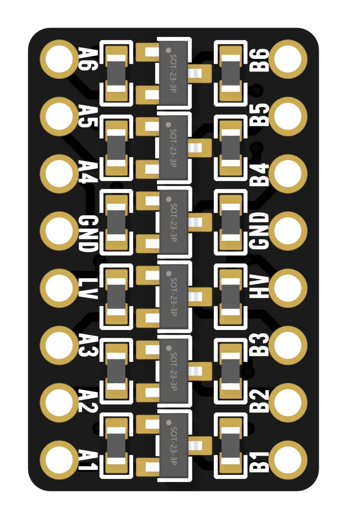
The two GND pins are the same copper. Wiring both is not required, but it is the easiest way to be sure both of your boards share a ground.
The 6-pack: two chips, one footprint
The TXB0108 and TXS0108 boards are identical from the outside: eight channels, VA and A1–A8 down one edge, VB and B1–B8 down the other. The chip in the middle is what differs, and the title on the silkscreen tells you which is which: TXB0108 [SPI] and TXS0108 [I2C].
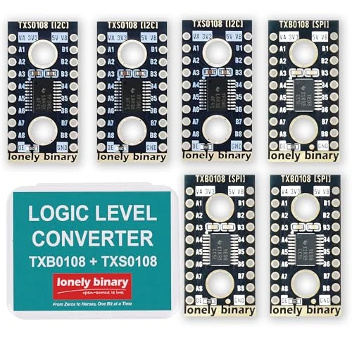
Two things are different from the MOSFET boards. There is one GND, bottom right on the B side. And the pin opposite it, bottom left, is OE, not a second ground. The next page is about both.
On a breadboard
The holes are on a 2.54 mm grid. With header pins fitted, each board straddles a breadboard's centre channel, A pins on one side and B pins on the other.
When it does not work
You are looking at the back. The pin names are printed on the component side, the one with the transistors or the chip on it. The back carries the product name and, on the TXB and TXS, the DISABLE: OE->GND reminder.
Either way works electrically. What matters is that the A row is wired to the 3.3 V board and the B row to the 5 V part. Turn the board so the A labels face your 3.3 V board and the wires stay short and uncrossed.
Leave the unused channels unconnected. On the MOSFET and TXS boards, pull-up resistors hold each unused channel at a steady level, so it does nothing by itself.
LV, HV and GND come first, and each of them fails differently when it is missing.
Power before signals →Edit this page — content/books/llc/the-five-boards.mdx
Questions about this product
See what other owners have asked, and read their solutions.
This page covers several products. Choose yours to see the right discussions.
Discuss this article
Ask about this page. The answer stays here, on the page it belongs to, for whoever hits the same wall next.