What is on it
Six BSS138 transistors, one per channel, each with a 10 kΩ pull-up to 3V3 on its L side and to 5V on its H side. An ME6211 regulator that makes the 3V3 from 5V, with 10 µF and 100 nF on each side of it. A socket, a header and two LEGO holes. No chip decides anything: every channel is three parts.
Three parts per channel, and a regulator
Six BSS138 transistors, five in a row across the middle and the sixth beside H6. Each one's gate is on 3V3, one side on its L pin and the other on its H pin. The data sheet says it switches on with 0.8 to 1.6 V on its gate, and it always has 3.3 V, so it switches fully.
Twelve 10 kΩ resistors, one from each L pin up to 3V3 and one from each H pin up to 5V. These make every HIGH on the board. Nothing else drives a line up, which is what makes the board work in both directions, and what sets its speed.
An ME6211 regulator, the five-legged part at the lower left. Its input and its enable pin are both on 5V, so it is on whenever 5V is, and its output is the 3V3 rail. Beside it, 10 µF and 100 nF on its input; at the upper left, the same pair on its output.
What is not on it
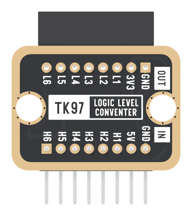
There is no chip, no direction pin and no enable pin. The llc book's TXB0108 and TXS0108 boards have an OE pin that switches every channel off; this board has nothing like it. There is no way to set the low side's voltage, either: 3.3 V is the regulator's, and a part that needs 1.8 V wants a different converter.
There is also no connection from the socket's 3V3 back to 5V except through the regulator. That one arrow, 5V in and 3V3 out, is what the 3V3 pin is an output is about.
When it does not work
The channels are: a BSS138 and two 10 kΩ each, as on the loose 6CH board. The difference is power. The 6CH board has LV and HV inputs you feed yourself; the TK97 takes only 5V and makes its own 3.3 V, so its 3V3 pin is an output.
It is Q6, channel 6's. It sits apart, beside H6, and is wired exactly like the other five: gate on 3V3, one side on L6, the other on H6.
No. The low side is fixed at 3.3 V by the regulator; there is no pin to set it. For 1.8 V use a converter whose low side you supply, such as the TXB0108 or TXS0108 boards in the llc book.
No. Every line already has a 10 kΩ pull-up on each side, and most I2C blocks bring their own as well.
How one transistor and two resistors pass a signal in either direction with no direction pin.
One channel, both ways →Edit this page — content/books/logic-level-converter/what-is-on-it.mdx
Questions about this product
See what other owners have asked, and read their solutions.
Logic Level Converter
Loading discussions…
Discuss this article
Ask about this page. The answer stays here, on the page it belongs to, for whoever hits the same wall next.