Specifications
| Type | Bidirectional level converter, MOSFET-based |
|---|---|
| Channels | Four, typical |
| High side | 5 V |
| Low side | 3.3 V |
| Speed | Fine for I2C and slow SPI; not for fast SPI |
What it is
Four MOSFETs with pull-ups, one per channel. Each channel passes a signal in either direction, shifting between the two voltages.
The reason it is needed: an ESP32, a Pico and a Raspberry Pi are 3.3 V parts, and their pins are not 5 V tolerant. A 5 V sensor output wired straight to one does not usually fail immediately — it damages the input protection slowly, which is why it looks like it works and then the board becomes flaky weeks later.
There is a low-side and a high-side, and they are not interchangeable. LV goes to the 3.3 V board, HV to the 5 V one, and both must be powered for the channels to work at all — a converter with only one side powered passes nothing and looks broken.
The MOSFET topology depends on the pull-ups to drive the line high, which makes it slower on rising edges. That is invisible on I2C at 100 kHz and becomes a real limit on SPI above a few megahertz, where you want a dedicated buffer instead.
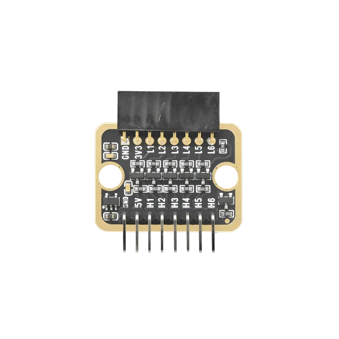
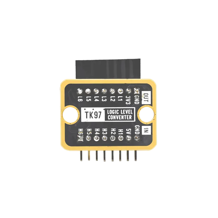
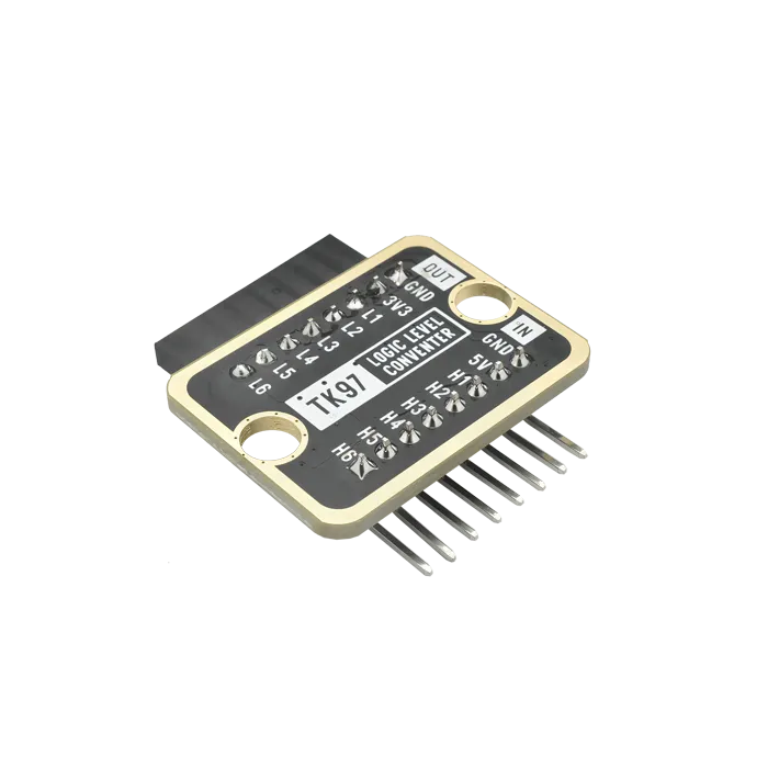
Pinout
OUT side - 3.3V side:
- GND (negative): Connect to 3.3V device's GND
- 3V3 (positive): Connect to 3.3V device's 3.3V power supply
- L1-L6 (channels 1-6): 6 bidirectional conversion channels, connect to 3.3V device's signal pins
IN side - 5V side:
- GND (negative): Connect to 5V device's GND
- 5V (positive): Connect to 5V device's 5V power supply
- H1-H6 (channels 1-6): 6 bidirectional conversion channels, connect to 5V device's signal pins
Wiring
- OUT side GND → 3.3V device GND
- OUT side 3V3 → 3.3V device 3.3V
- IN side GND → 5V device GND
- IN side 5V → 5V device 5V
- OUT side L1 → 3.3V device signal pin
- IN side H1 → 5V device signal pin
When it doesn’t work
- Nothing gets through.
- Both sides need power. LV to 3.3 V, HV to 5 V, and grounds tied together — all three, not two.
- It works on I2C and not on fast SPI.
- The pull-up drives the rising edge, so the signal is slew-limited. Slow the clock, or use a push-pull buffer.
- Do I need it for an input the other way?
- Yes, in both directions — the channels are bidirectional, but the 3.3 V pin still must never see 5 V.