The adapter, pin by pin
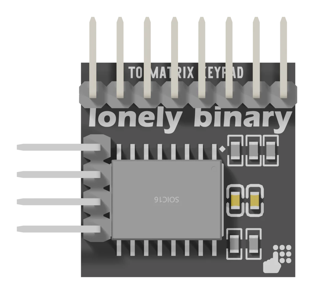
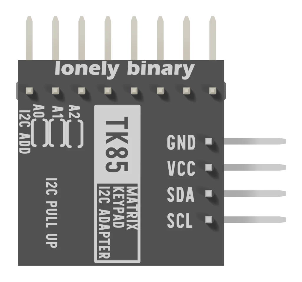
Twenty millimetres square, one chip, and four jobs: eight pins for the keypad, four for your board, three pads that set the address, and one pad that removes the pull-ups. Two of the pad labels on the back are the wrong way round.
Both sides
Four jobs
Every part on the board belongs to one of four jobs. Pick one to light it, and turn the board over for the two that live on the back.
P7 → chip pin 12 · P6 → chip pin 11 · P5 → chip pin 10 · P4 → chip pin 9 · P3 → chip pin 7 · P2 → chip pin 6 · P1 → chip pin 5 · P0 → chip pin 4
The keypad header is eight pins wired straight to the chip's P0 to P7, with nothing in between. Seen from the front with the header at the top, they run P7 on the left to P0 on the right.
The bus header is GND, VCC, SDA and SCL, top to bottom. The chip runs on 2.5 to 6 V. Feed VCC from your board's own logic voltage — 3.3 V on an ESP32, 5 V on an Uno — because the next job ties SDA and SCL to it.
The pull-ups are two 10 kΩ resistors from SDA and SCL to VCC. I²C needs them: devices on the bus only ever pull the lines down, and something has to pull them back up. They reach VCC through the pad printed I2C PULL UP. Cutting the thin trace between its two halves removes them, which matters only when many boards share one bus.
The address pads are three pairs of pads, one per address bit. Each address pin is held at 0 by a 10 kΩ resistor to GND; a blob of solder across a pad connects it to VCC instead and makes that bit 1.
The two labels that are swapped
The design files and the silkscreen disagree. The pad printed A0 is wired to the chip's A2 pin, and the pad printed A2 to A0. A1 is right.
So bridging the pad marked A0 moves the adapter from 0x20 to 0x24, not 0x21. Nothing is harmed — it is still a different address, which is the point — but do not trust the arithmetic. After soldering, scan the bus and use the address it prints. More than one keypad walks through it.
When it does not work
Not on this adapter. The PCF8574 has an INT output, and the I2CKeyPad library can use it, but the adapter does not bring it out to a pin. Poll every 20 ms or so; it costs well under a millisecond each time.
A 10 µF and a 100 nF capacitor across the supply. They hold VCC steady at the chip while it switches, and they need nothing from you.
The chip does not need them. A PCF8574 pin set to 1 is held high only by a weak current source of tens to hundreds of microamps, which a pressed key can overpower; a pin set to 0 pulls down hard. The next chapter shows why that is enough to read a key.
It is a different board outline with the same job. Its photos show the pull-up pad on the back; if yours also has pads marked A0 to A2, the advice here applies to it, and a bus scan is the check either way.
How the library finds a pressed key with two writes and two reads, and why the answer is a number, not a character.
Two reads per key →Edit this page — content/books/matrix-keypad/the-adapter-pin-by-pin.mdx
Questions about this product
See what other owners have asked, and read their solutions.
This page covers several products. Choose yours to see the right discussions.
Discuss this article
Ask about this page. The answer stays here, on the page it belongs to, for whoever hits the same wall next.