The eight pins
Eight pins: 3V3 and GND for power, SCL and MOSI for the SPI clock and data, CS, DC and RST for the controller, and BL, which switches the backlight rather than powering it. Five of them go straight to the panel's ribbon with nothing in between. No pad is square, so count from the names.
Two names for each pin
The header is eight right-angle pins, 2.54 mm apart, down the short edge to the left of the screen. The front prints short names beside the pads: BL, RST, DC, SCL, MO, CS, 3V3, GND from the top. The back prints the same pins in full: BACKLIGHT, RST, DC, SCL, MOSI, CS, 3V3, GND. MO and MOSI are one pin.
Pick a pin to see where it goes. 3V3 and GND feed the panel, its controller and its backlight. SCL and MOSI are SPI's clock and data, from your board to the display and never back. CS, DC and RST are the controller's three control lines. BL switches the backlight.
Straight to the ribbon
RST, DC, SCL, MOSI and CS each go to one contact of the socket that holds the panel's ribbon, and to nothing else: no resistor, no pull-up, no level shifter. What your board puts on those pins is what the panel's controller gets. That is why the 3.3 V rule matters so much here.
BL is the exception. It goes to the gate of a small transistor that switches the backlight, with a 10 kΩ resistor to GND. Leave it unwired and the backlight stays off. The backlight waits for BL is about that.
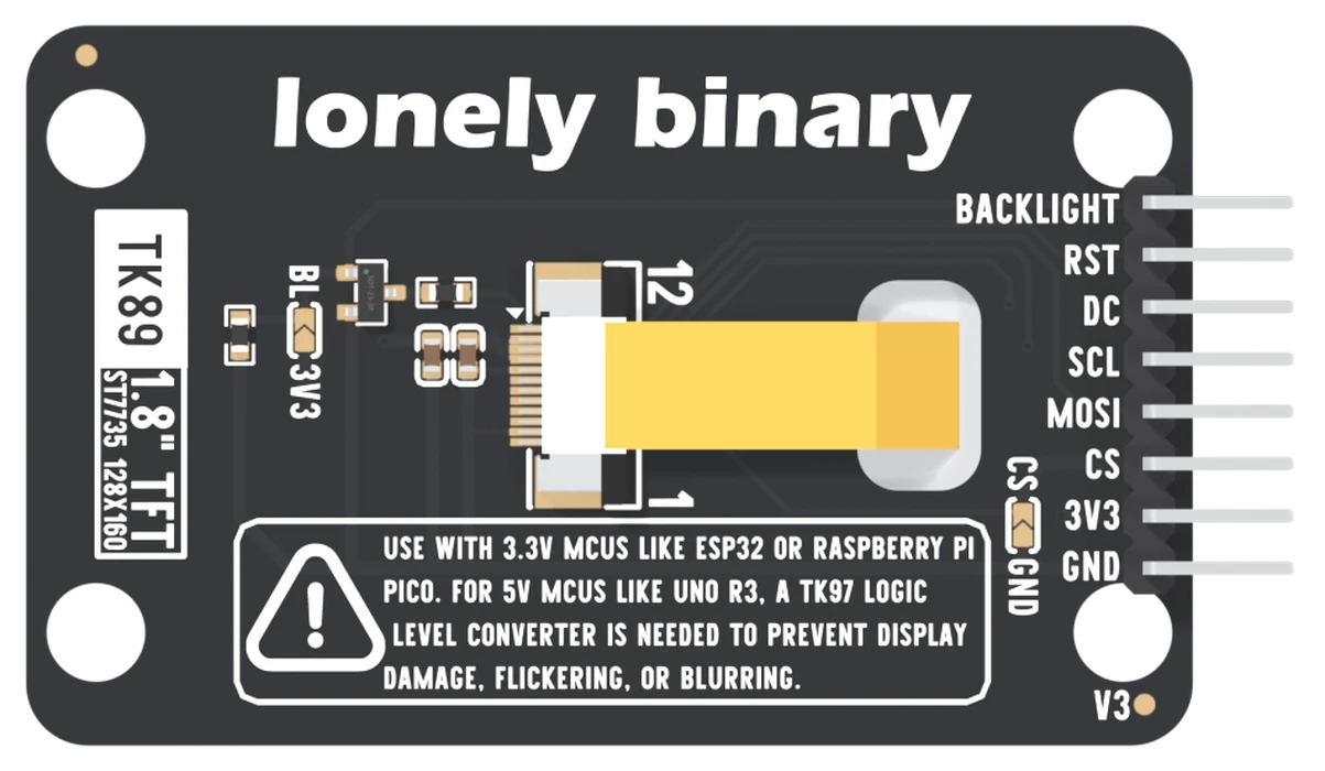
No square pad
On most TinkerBlock blocks the square pad marks GND. Here all eight pads are round, so there is nothing to count from but the names. With the screen facing you and the header on the left, GND is at the bottom. Turned over, it is still at the bottom.
When it does not work
With the screen facing you and the header on the left, GND is the bottom pin and BL the top one. The front prints BL RST DC SCL MO CS 3V3 GND top to bottom; the back prints the same order in full, starting with BACKLIGHT. All eight pads are round, so the names are the only guide.
No. On this board SCL is the SPI clock, the pin your board's pinout calls SCK or SCLK. Wiring it to your board's I2C SCL does nothing useful. There is no I2C on the TK89 at all.
No. The board has no MISO pin: nothing ever comes back from the display. SCL and MOSI are the only SPI wires, plus CS, DC and RST from any spare outputs.
Only if you have bridged the BL-3V3 jumper on the back. Otherwise a 10 kOhm resistor on the board holds the backlight off, and the display looks dead however well the rest is wired.
A ribbon socket, a transistor for the backlight, two capacitors, two jumpers, and glass that is 1.77 inches.
What is on it →Edit this page — content/books/tft-1-8-inch/the-eight-pins.mdx
Questions about this product
See what other owners have asked, and read their solutions.
1.8-inch TFT Display
Loading discussions…
Discuss this article
Ask about this page. The answer stays here, on the page it belongs to, for whoever hits the same wall next.