Which pin is which
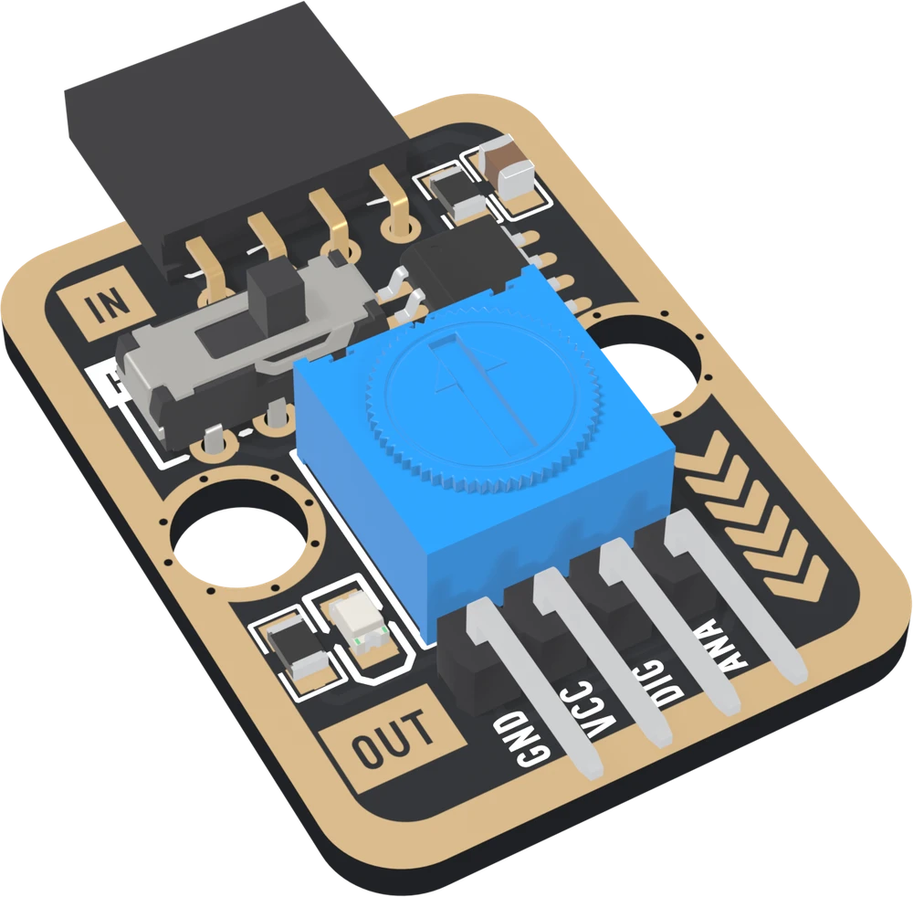
OUT prints GND, VCC, DIG and ANA, GND on the square pad. IN prints nothing, and takes a block's GND, VCC, NC and SIGNAL in the same order. Three of OUT's pins are the same copper as three of IN's: only DIG is new, and it sits where a sensor block has NC.
OUT, from the square pad
Parts up and OUT at the bottom, the pins read GND, VCC, DIG, ANA from left to right, and the names are printed along them. GND is on the square pad.
GND and VCC power the whole thing: the comparator, the knob, the LED, and the block in the IN socket, which gets its supply through the TK29.
DIG is the comparator's output: HIGH or LOW. It goes to a digital input on your board.
ANA is not an input. The net list puts it on the same net as the IN socket's fourth position, so it is the block's SIGNAL carried straight through. Wire it to an analog input if you want the number as well as the decision; leave it unconnected if you do not.
IN, in a block's order
The socket prints only IN beside it. Its four positions, left to right, are GND, VCC, nothing, and the input: the same order as every TinkerBlock sensor's header, GND, VCC, NC, SIGNAL. So a block plugs in with its parts facing the same way as the TK29's, and each of its pins meets the right one.
The third position is in no net at all. It is where the block's NC lands, so nothing is lost.
Why DIG is third
Put a sensor block's header beside OUT and compare. GND, VCC and SIGNAL line up with GND, VCC and ANA; where the block has NC, the TK29 has DIG. That is the design: OUT is the block's own header with the unused pin put to work.
It also means VCC has to be your board's logic voltage. DIG is pulled up to VCC, and the block's SIGNAL can reach VCC too, so 3V3 beside an ESP32, ESP32-S3 or Pico, and 5V beside an Uno.
The back
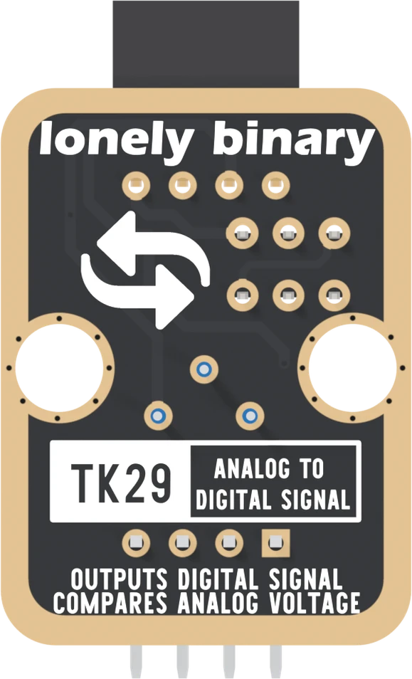
The back prints the part number and what it does, and no pin names. Turned over, the order reverses: the square pad is on the right, and it is still GND.
When it does not work
Hold the board with the parts facing you and OUT at the bottom. Read GND, VCC, DIG, ANA from left to right; the names are printed along the pins. GND is also the square pad, which is the mark that survives once the board is in a breadboard.
Parts facing the same way as the TK29's, the block above it, its pins pushed down into the socket. Then the block's GND meets the socket's left-hand position and its SIGNAL the right-hand one, which is what the board expects. Backwards, the block's GND lands on the TK29's SIGNAL position and nothing works.
It would work electrically, because ANA and IN's fourth position are the same copper. But the block would get no power from that one wire, so you would be wiring GND and VCC to it separately. IN exists so you do not have to.
No. It prints TK29, ANALOG TO DIGITAL SIGNAL and two lines about what it does. Turned over, OUT's square pad is on the right, and it is still GND.
What the comparator does with the two voltages, and what the answer cannot tell you.
Two inputs, one answer →Edit this page — content/books/analog-to-digital-signal/which-pin-is-which.mdx
Questions about this product
See what other owners have asked, and read their solutions.
Analog to Digital Signal
Loading discussions…
Discuss this article
Ask about this page. The answer stays here, on the page it belongs to, for whoever hits the same wall next.