The two rows
Two rows of eight, one along each long edge. The socket's row is the 3.3 V side, GND, 3V3 and L1 to L6; the header's row is the 5 V side, GND, 5V and H1 to H6. Each L pin sits straight above the H pin of the same number, and those two are one channel.
One row for each voltage
Hold the board with the black socket at the top. The socket's row is the 3.3 V side: GND, 3V3, then L1 to L6. The header's row along the bottom is the 5 V side: GND, 5V, then H1 to H6. L is for low, H for high.
Pick a channel. Ln is straight above Hn, and the transistor between them is the whole channel: a signal that goes in at one end comes out at the other, moved to the other side's voltage. Six channels means six signals, enough for an SPI display with its reset, data/command and backlight lines.
Pick 5V and 3V3. They are not a pair of inputs. 5V is the board's only supply; 3V3 is made on the board, from 5V, and comes out of the socket for a 3.3 V block to use. The 3V3 pin is an output says why that decides the wiring.
Start at GND, not at the square pad
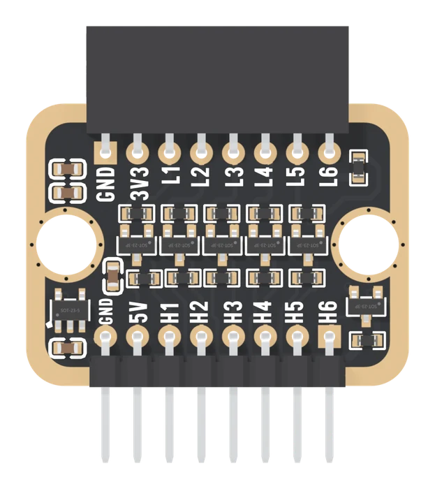
Both rows start at GND at the left, and the two GND pins are one connection on the board. The square pads do not agree: the socket's is GND, but the header's is H6, at the far right. Count from the printed name.
The socket takes a block's right-angle header straight in, so a 3.3 V block plugs into the TK97 without wires. The header takes jumper wires, or a female socket, from the 5 V board.
Which side your board goes on
- A 5 V board, such as an Uno, goes on the header: 5V, GND and its signals on H1 to H6. The 3.3 V block goes in the socket.
- A 3.3 V board, such as an ESP32 or a Pico, goes on the socket's side: GND and its signals on L1 to L6, and its 5V pin round to the header's 5V. The 5 V part goes on H1 to H6.
Either way the board needs 5V and GND, and nothing on your side is ever wired to the socket's 3V3 except a 3.3 V block that takes power from it.
When it does not work
The back prints the same names, mirrored, with OUT beside the socket's row and IN beside the header's. OUT is the 3.3 V side, L1 to L6 and 3V3; IN is the 5 V side, H1 to H6 and 5V.
The two rows put their square pads at opposite ends. On the socket's row it is GND, at the left with the socket at the top; on the header's row it is H6, at the right. Both rows start at GND at the left, so count from the name GND, not from the square.
There are six: L1 to L6 and H1 to H6, one transistor each. The page this book replaces said four, and named LV and HV pins the board does not have. Wire by the names printed on the board.
Six transistors, twelve 10 kΩ resistors, a regulator and four capacitors.
What is on it →Edit this page — content/books/logic-level-converter/the-two-rows.mdx
Questions about this product
See what other owners have asked, and read their solutions.
Logic Level Converter
Loading discussions…
Discuss this article
Ask about this page. The answer stays here, on the page it belongs to, for whoever hits the same wall next.