What is on the board
Two screw terminals for the rail you are measuring, a four-pin header for your microcontroller, and between them a 100 mΩ shunt, the INA219, three capacitors, four 10 kΩ resistors and a red LED. Everything except the header carries the rail; the header carries I²C and the chip's own supply.
One block, assembled
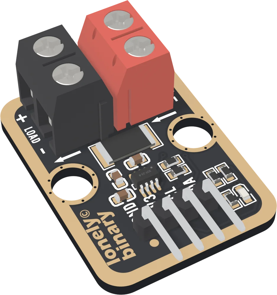
The block arrives with both terminals and the right-angle header soldered on. It is the standard TinkerBlock size, 22.4 × 30.4 mm, with two LEGO-compatible holes.
The rail, at the top
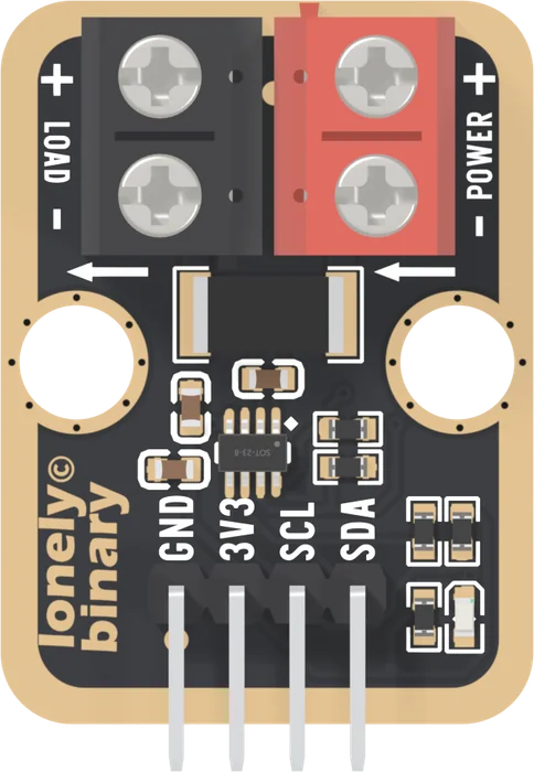
| Screw | Connected to | Wire it to |
|---|---|---|
| POWER + | One end of the shunt, the chip's IN+ | The supply's positive |
| POWER − | Ground | The supply's negative |
| LOAD + | The shunt's other end, the chip's IN− | The load's positive |
| LOAD − | Ground | The load's negative |
The two + screws are the two ends of the shunt. The two − screws are the same wire, and that wire is also the header's GND.
The header, at the bottom
| Pin | The chip calls it | Wire it to |
|---|---|---|
| GND | GND | GND |
| 3V3 | VS, its supply | Your board's logic supply, 3 to 5.5 V |
| SCL | SCL | Your SCL pin — the third pin |
| SDA | SDA | Your SDA pin |
The clock comes before the data on this board, which is the other way round from most I²C boards. SCL comes first is the page about it.
The parts between
The chip is a Texas Instruments INA219AIDCNR, the A grade, in an eight-legged SOT-23 package. The shunt is a Yageo 2512 resistor, 100 mΩ within 1 %, rated 2 W.
The rest are small. Two 10 kΩ resistors pull SCL and SDA up to the 3V3 hole; two more hold the chip's address pins at ground until a pad on the back is bridged. A 10 µF and a 100 nF capacitor steady the chip's supply, and a third, 100 nF, sits straight across the shunt's two ends. The red LED lights from 3V3 through 5.1 kΩ, about a quarter of a milliamp.
The back
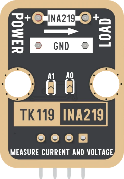
Seen from behind, the board is mirrored, so POWER is on the left and the arrow points right. The two pads marked A1 and A0 set the address; Four addresses says how.
When it does not work
The red one, marked POWER, takes the supply. The black one, marked LOAD, goes to the thing drawing the current. The arrows printed between them point from POWER to LOAD, which is the way current must flow for the reading to be positive. On the back, POWER and LOAD are printed the other way round because the board is flipped.
The LED only says the header's GND and 3V3 are connected. It runs from the 3V3 hole through 5.1 kΩ and is not driven by the chip, so it lights whether or not the INA219 is answering, and whether or not the rail is connected. SCL and SDA are the next thing to check.
Yes. POWER −, LOAD − and the header's GND are one copper net on this board. That is why the supply you measure and the board reading it end up sharing a ground, and why the block cannot go in a negative wire.
They are through-hole parts soldered on at the factory. Desoldering a five-millimetre-pitch terminal is possible but slow, and the pads are sized for its pins. Wires screwed in are the intended connection.
Where the block goes in a circuit, and the three places that look right and are not.
POWER in, LOAD out →Edit this page — content/books/ina219/whats-on-the-board.mdx
Questions about this product
See what other owners have asked, and read their solutions.
TK119 INA219 Current and Voltage Monitor
Loading discussions…
Discuss this article
Ask about this page. The answer stays here, on the page it belongs to, for whoever hits the same wall next.