The four pins
Four pins, and one of them is a limit rather than a choice: 3V3 means 3.3 V, because the chip's absolute maximum is 3.6 V. Around the pins are the two pull-ups, two capacitors and a power light that somebody has already fitted for you.
The four names
Chip side up, header at the bottom, the silkscreen reads GND, 3V3, SCL and SDA from left to right. GND is the square pad.
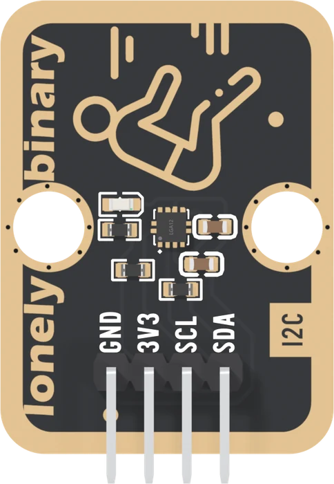
GND is the return for everything. Connect it first.
3V3 is the supply, and the name is a limit. The SC7A20H runs from 1.71 V to 3.6 V, and 3.6 V is also its absolute maximum: the voltage past which the data sheet stops promising the chip survives. There is no regulator on this board, so what you put on this pin is what the chip gets. 5 V is out.
SCL and SDA are the I²C bus, clock and data. Both are shared with any other I²C device on the project.
What else is soldered to it
Six small parts sit round the chip. Pick a group to see which is which:
- R7 and R8, 4.7 kΩ, pull SCL and SDA up to 3V3. Every device on an I²C bus only ever pulls a line down; something has to pull it back up, and here it is fitted. They are always connected. There is no jumper.
- C1 and C2, 100 nF each, sit across the supply. They hold the voltage steady for the moment the chip draws a burst of current, which a long wire from your board cannot.
- LED1 and R6, 1 kΩ, are the power light. It is on whenever 3V3 is, and it draws about 1.3 mA doing it, some eighty times what the chip draws at 100 readings a second. It does not blink when a reading is taken.
Why the pull-ups decide the voltage
Because R7 and R8 go to 3V3, the bus idles at whatever the 3V3 pin is fed. On an ESP32, an ESP32-S3 or a Pico that is 3.3 V and correct, and their pins are made for it.
A 5 V Arduino Uno is the awkward one. Its pins can read 3.3 V as high, but its Wire library also turns on its own pull-ups, to 5 V, and those lift the idle lines towards the chip's limit. The first reading puts a level converter in between for an Uno, and explains the numbers.
The chip in the middle
The accelerometer is the 2 mm square between the mounting holes, in an LGA package: twelve pads underneath and no legs at all. Six of the twelve are wired: SDA, SCL, two supply pins and two ground pins. The other six are left open, and four of those decide something about the board. That is the pins left open.
When it does not work
Hold the board chip side up with the header at the bottom and read GND, 3V3, SCL, SDA from left to right. GND is on the square pad, which you can see on the back. The back prints the four names mirrored, the usual way SDA and SCL end up swapped.
No. The chip is rated for 3.6 V at most on its supply, and 5 V is well past it. The board has no regulator: whatever goes into 3V3 goes straight to the chip. Use your board's 3.3 V pin.
The light only proves 3V3 and GND arrived. It sits straight across the supply through a 1 kΩ resistor and knows nothing about the bus. A lit board that does not answer is almost always SDA and SCL swapped, or no ground shared with the host.
No. R7 and R8, 4.7 kΩ each, pull SCL and SDA up to 3V3 on the board, and there is no jumper to take them off. With several I²C boards on one bus their pull-ups add in parallel. Four boards like this one come to about 1.2 kΩ, which asks a device to sink 2.8 mA, still inside the 3 mA the I²C standard allows.
Three arrows nobody printed on the board, and how to find them in ten seconds.
Which way is X →Edit this page — content/books/3-axis-accelerometer/the-four-pins.mdx
Questions about this product
See what other owners have asked, and read their solutions.
3-Axis Accelerometer
Loading discussions…
Discuss this article
Ask about this page. The answer stays here, on the page it belongs to, for whoever hits the same wall next.