Specifications
| Display | 8 x 8 pixels, 64 LEDs in one package, a single fixed colour per board |
|---|---|
| Driver | One MAX7219. It holds the image in its own memory and scans it, so your board sends a frame and then has nothing more to do |
| Boards | Two. The TK52 has one 6-way header and no DOUT pad. The chainable module has six pads at each of two opposite edges, marked IN and OUT |
| Header | GND, VCC, CS, DIN or DOUT, NC, CLK. Fitted on the TK52, supplied loose with the 3-pack |
| Signal wires | 3 — DIN, CLK and CS — however many boards are chained |
| Supply voltage | 5 V. The MAX7219's operating range is 4.0 to 5.5 V, so 3.3 V is outside it |
| Logic level | A HIGH must reach 3.5 V. A 5 V board clears it; a 3.3 V board is below the datasheet minimum and usually works anyway |
| Brightness | 16 levels, set in software. A duty cycle from 1/32 to 31/32, not a change in LED current |
| Scan rate | 800 Hz typical with all eight columns scanned, 500 to 1300 Hz specified |
| Clock | 10 MHz maximum, which is a 100 ns minimum clock period |
| Current | 330 mA typical with every LED lit at full brightness, 150 µA in shutdown. Tens of milliamps for an icon at a normal setting |
| In the box | The 3-pack holds 3 modules, one each in red, green and blue, with a colour-matched case and a set of headers for each. The TK52 ships singly and in the TinkerBlock kits |
| Module size | 3.2 x 3.2 x 1.0 cm for the chainable module, measured without its case |
What it is
Sixty-four LEDs and a driver that scans them fast enough to look continuous. You write eight bytes — one per row — and the chip holds the image. Send a frame, unplug the data wire, and the picture stays.
The driver is a MAX7219. It does the multiplexing, the constant-current drive and the brightness, and it takes its instructions as sixteen-bit messages on three wires: data, clock, and chip select. Brightness is sixteen steps of duty cycle, from 1/32 to 31/32 — the chip dims the display by lighting it for less of each scan, not by pushing less current through the LEDs.
It wants 5 V. The MAX7219's operating range is 4.0 to 5.5 V, so 3.3 V is below it. The signals are a separate question: a HIGH has to reach 3.5 V, which a 3.3 V board misses by two tenths of a volt. Driving one of these from an ESP32 is common, usually works, and is outside the datasheet either way.
Text needs a font, and a font is 8 bytes per character. The MD_MAX72XX and
LedControl libraries include one; rolling your own is a fun afternoon and not
otherwise necessary.
Two boards, one chip
The same chip sits behind two different Lonely Binary boards, and the difference between them is one pad.
The TK52 is the TinkerBlock part. The matrix is at the top, there is a single
six-way header along the bottom edge with the pins already fitted, and the back
reads TK52 MATRIX LED. Its six pads are CLK, NC, DIN, CS, VCC, GND. There is no
DOUT anywhere on it, so a TK52 talks to your board and to nothing else.
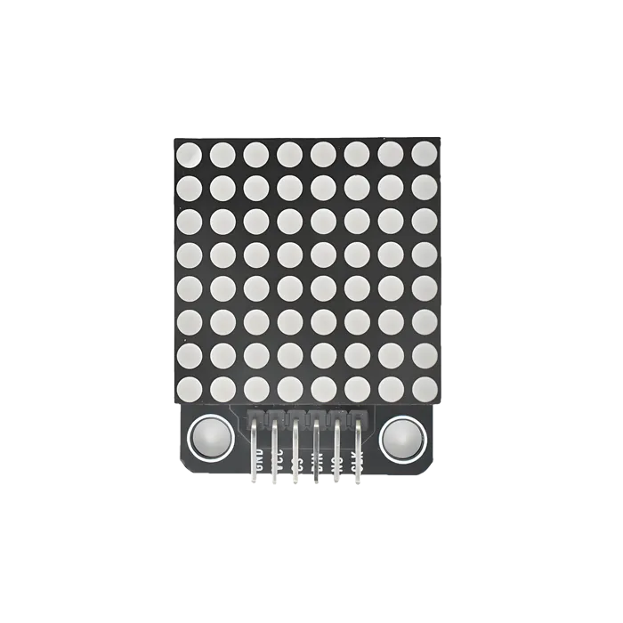
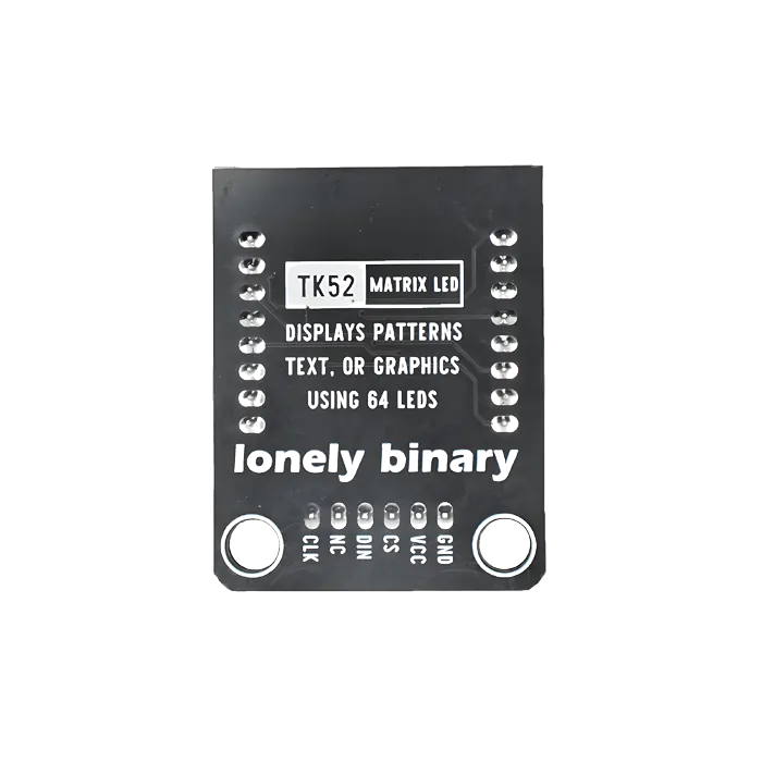
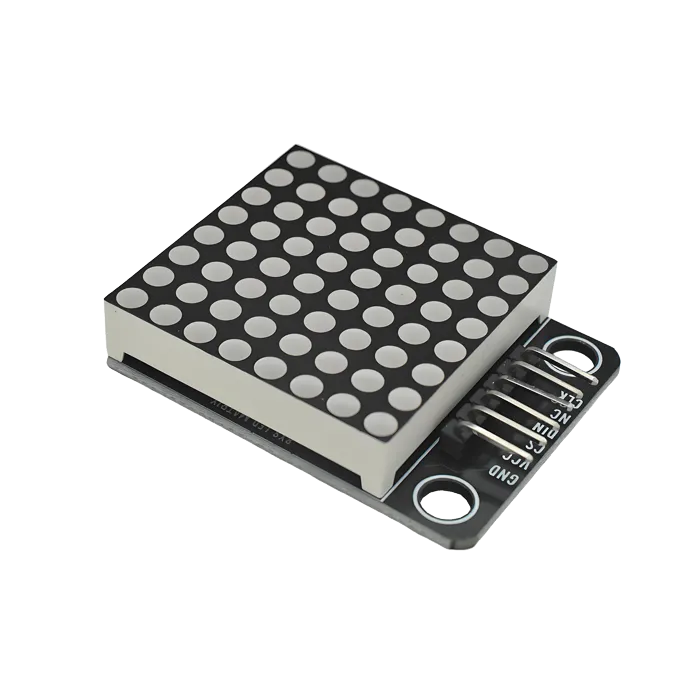
The chainable module is the one that comes three to a box, in red, green and blue. It is a 3.2 cm square, and it has six pads at each of two opposite edges. One edge is marked IN and carries DIN; the other is marked OUT and carries DOUT. The two edges are otherwise the same six pads in the same order, which is what makes a chaining jumper a straight six-way run.
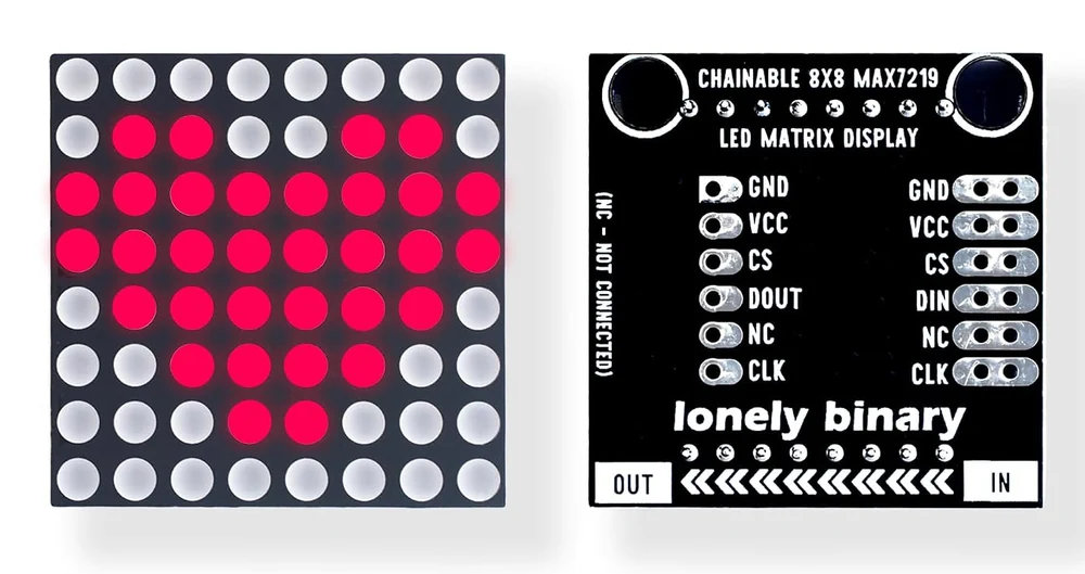
The arrows on the back run from IN towards OUT. That is the direction the data travels, and it is the one thing on the board worth reading before you solder.
Pinout
- GND (negative): Like the negative terminal (-) of a battery, connect to the control board's GND
- VCC (positive): Like the positive terminal (+) of a battery, connect to the control board's 5V (this module requires 5V power supply)
- CS (chip select): SPI chip select signal, connect to the control board's digital pin (e.g. Arduino D10 or Pico GPIO 5)
- DIN (data input): SPI data input pin, connect to the control board's SPI data pin (e.g. Arduino D11 or Pico GPIO 19)
- NC (no connection): No actual circuit connection, included for unified interface, can be left unconnected
- CLK (clock): SPI clock signal, connect to the control board's SPI clock pin (e.g. Arduino D13 or Pico GPIO 18)
On the chainable module the same six names appear at both edges. The IN edge is the one above; on the OUT edge the fourth pad is DOUT instead of DIN, and that is the only difference. Wire your microcontroller to IN. A controller wired to OUT gets nothing through, because DOUT is the chip talking rather than listening.
Wiring
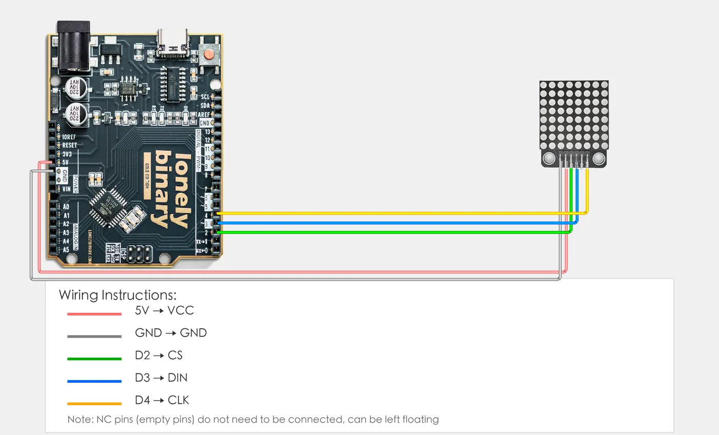
- GND → Control board GND
- VCC → Control board 5V
- CS → Control board digital pin (e.g. D10)
- DIN → Control board SPI data pin (e.g. D11)
- CLK → Control board SPI clock pin (e.g. D13)
Chaining
Chaining is serial. DOUT of one module goes to DIN of the next, while VCC, GND,
CLK and CS run straight through to every board in the line. The three signal
wires back to your microcontroller do not change however many boards you add.
What changes is the number the sketch declares — four chained modules is
LedControl(DIN, CLK, CS, 4), and a sketch that still says 1 lights one square
and leaves the rest dark.
Each chip passes the sixteen bits it has already received out of DOUT, 16.5 clock cycles behind DIN. So the packet you send first travels furthest, and the module nearest your board ends up holding the packet you sent last. A picture that turns up one board along from where you wanted it is a counting error, not a wiring fault.
Only the chainable module can do this at all. The TK52 brings out no DOUT pad.
The 3-pack ships its headers loose, and the listing is straight about what that means: joining two modules is a soldering job. The listing puts the practical limit at eight modules in a line. Nothing in the protocol stops you there — what does not scale is current, because a chained board draws everything it needs through its neighbour's VCC pad. Two on one jumper is fine at a normal brightness; past that, run 5 V and ground to each board from the supply.
Example
#include <LedControl.h>

// Pin number: change these to match your wiring
// Demo program uses: DIN=3, CLK=4, CS=2
// If using hardware SPI: DIN=11(MOSI), CLK=13(SCK), CS=10
// If using software SPI: can use any digital pins
#define CS_PIN 2    // Arduino digital pin connected to CS (demo uses D2)
#define DIN_PIN 3   // Arduino digital pin connected to DIN (demo uses D3)
#define CLK_PIN 4   // Arduino digital pin connected to CLK (demo uses D4)

// 8×8 matrix LED configuration (using MAX7219 driver, LedControl library supports software SPI)
// Note: the last argument is the number of 8×8 modules on the chain, not the number of boards
// LedControl constructor: LedControl(dataPin, clockPin, csPin, numDevices)
LedControl lc = LedControl(DIN_PIN, CLK_PIN, CS_PIN, 1);  // Single 8×8 module

// Pattern data (8×8 dot matrix, each pattern 8 bytes)
// Heart pattern
const byte heartPattern[8] = {
  0b00000000,
  0b01100110,
  0b11111111,
  0b11111111,
  0b11111111,
  0b01111110,
  0b00111100,
  0b00011000
};

// Triangle pattern
const byte trianglePattern[8] = {
  0b00000000,
  0b00010000,
  0b00111000,
  0b01111100,
  0b11111110,
  0b01111100,
  0b00111000,
  0b00010000
};

// Square pattern
const byte squarePattern[8] = {
  0b11111111,
  0b10000001,
  0b10000001,
  0b10000001,
  0b10000001,
  0b10000001,
  0b10000001,
  0b11111111
};

// Circle pattern
const byte circlePattern[8] = {
  0b00111100,
  0b01111110,
  0b11000011,
  0b10000001,
  0b10000001,
  0b11000011,
  0b01111110,
  0b00111100
};

// Star pattern
const byte starPattern[8] = {
  0b00011000,
  0b00111100,
  0b01111110,
  0b11111111,
  0b01111110,
  0b00111100,
  0b00011000,
  0b00000000
};

// Arrow pattern
const byte arrowPattern[8] = {
  0b00001000,
  0b00011100,
  0b00111110,
  0b01111111,
  0b00011100,
  0b00011100,
  0b00011100,
  0b00000000
};

// Smile pattern
const byte smilePattern[8] = {
  0b00111100,
  0b01000010,
  0b10100101,
  0b10000001,
  0b10100101,
  0b10011001,
  0b01000010,
  0b00111100
};

// Pattern array for easy looping
const byte* patterns[] = {
  heartPattern,      // 0: Heart
  trianglePattern,   // 1: Triangle
  squarePattern,     // 2: Square
  circlePattern,     // 3: Circle
  starPattern,       // 4: Star
  arrowPattern,      // 5: Arrow
  smilePattern       // 6: Smile
};

const char* patternNames[] = {
  "Heart",
  "Triangle",
  "Square",
  "Circle",
  "Star",
  "Arrow",
  "Smile"
};

const int patternCount = 7;  // Number of patterns

// Reverse byte bit order (fix mirror display issue)
byte reverseByte(byte b) {
  byte result = 0;
  for (int i = 0; i < 8; i++) {
    result <<= 1;
    result |= (b & 1);
    b >>= 1;
  }
  return result;
}

// Display pattern
void displayPattern(const byte* pattern) {
  // Clear display
  lc.clearDisplay(0);

  // Display pattern (reference demo program implementation)
  // Reverse byte bit order to fix mirror display issue
  for (int i = 0; i < 8; i++) {
    byte reversedByte = reverseByte(pattern[i]);
    lc.setRow(0, i, reversedByte);
  }
}

void setup() {
  // Initialize serial communication
  Serial.begin(9600);
  delay(100);

  Serial.println("8×8 matrix LED program started");
  Serial.println("Cycling through various patterns: Heart, Triangle, Square, Circle, Star, Arrow, Smile");

  // Initialize matrix LED (LedControl library)
  lc.shutdown(0, false);  // Wake up module 0
  lc.setIntensity(0, 8);  // Set brightness (0-15)
  lc.clearDisplay(0);     // Clear display
  delay(500);
}

void loop() {
  // Cycle through all patterns
  for (int i = 0; i < patternCount; i++) {
    displayPattern(patterns[i]);
    Serial.print("Display pattern: ");
    Serial.println(patternNames[i]);
    delay(1000);  // Switch pattern every second
  }
}from machine import Pin, SPI
import time
# Pin number: change these to match your wiring
CS_PIN = 5 # GPIO connected to CS (e.g. GPIO 5)
DIN_PIN = 19 # GPIO connected to DIN (e.g. GPIO 19, SPI data)
CLK_PIN = 18 # GPIO connected to CLK (e.g. GPIO 18, SPI clock)
# MAX7219 register addresses
REG_NOOP = 0x00
REG_DECODE = 0x09
REG_INTENSITY = 0x0A
REG_SCAN_LIMIT = 0x0B
REG_SHUTDOWN = 0x0C
REG_DISPLAY_TEST = 0x0F
# Initialize SPI and CS pin
# Pico SPI pin mapping:
# SPI0: SCK=GPIO18, MOSI=GPIO19, MISO=GPIO16
spi = None
if CLK_PIN == 18 and DIN_PIN == 19:
spi = SPI(0, baudrate=10000000, polarity=0, phase=0, sck=Pin(CLK_PIN), mosi=Pin(DIN_PIN))
else:
try:
spi = SPI(0, baudrate=10000000, polarity=0, phase=0, sck=Pin(CLK_PIN), mosi=Pin(DIN_PIN))
except:
spi = SPI(1, baudrate=10000000, polarity=0, phase=0, sck=Pin(CLK_PIN), mosi=Pin(DIN_PIN))
cs = Pin(CS_PIN, Pin.OUT)
cs.value(1) # CS HIGH
# Pattern data (8×8 dot matrix, each pattern 8 bytes)
# Heart pattern
heart_pattern = [
0b00000000,
0b01100110,
0b11111111,
0b11111111,
0b11111111,
0b01111110,
0b00111100,
0b00011000
]
# Triangle pattern
triangle_pattern = [
0b00000000,
0b00010000,
0b00111000,
0b01111100,
0b11111110,
0b01111100,
0b00111000,
0b00010000
]
# Square pattern
square_pattern = [
0b11111111,
0b10000001,
0b10000001,
0b10000001,
0b10000001,
0b10000001,
0b10000001,
0b11111111
]
# Circle pattern
circle_pattern = [
0b00111100,
0b01111110,
0b11000011,
0b10000001,
0b10000001,
0b11000011,
0b01111110,
0b00111100
]
# Star pattern
star_pattern = [
0b00011000,
0b00111100,
0b01111110,
0b11111111,
0b01111110,
0b00111100,
0b00011000,
0b00000000
]
# Arrow pattern
arrow_pattern = [
0b00001000,
0b00011100,
0b00111110,
0b01111111,
0b00011100,
0b00011100,
0b00011100,
0b00000000
]
# Smile pattern
smile_pattern = [
0b00111100,
0b01000010,
0b10100101,
0b10000001,
0b10100101,
0b10011001,
0b01000010,
0b00111100
]
# Pattern array for easy looping
patterns = [
heart_pattern, # 0: Heart
triangle_pattern, # 1: Triangle
square_pattern, # 2: Square
circle_pattern, # 3: Circle
star_pattern, # 4: Star
arrow_pattern, # 5: Arrow
smile_pattern # 6: Smile
]
pattern_names = [
"Heart",
"Triangle",
"Square",
"Circle",
"Star",
"Arrow",
"Smile"
]
pattern_count = 7 # Number of patterns
# Reverse byte bit order (fix mirror display issue)
def reverse_byte(b):
"""Reverse byte bit order"""
result = 0
for i in range(8):
result <<= 1
result |= (b & 1)
b >>= 1
return result
# Send command to MAX7219
def max7219_write(register, data):
"""Write data to MAX7219"""
cs.value(0) # CS LOW
# MAX7219 requires 16-bit data: high 8 bits are register address, low 8 bits are data
spi.write(bytes([register, data]))
cs.value(1) # CS HIGH
# Initialize MAX7219
def max7219_init():
"""Initialize MAX7219 chip"""
max7219_write(REG_DISPLAY_TEST, 0x00) # Disable display test
max7219_write(REG_SCAN_LIMIT, 0x07) # Scan all 8 rows
max7219_write(REG_DECODE, 0x00) # No BCD decode
max7219_write(REG_SHUTDOWN, 0x01) # Normal mode (0x00=shutdown, 0x01=on)
max7219_write(REG_INTENSITY, 0x08) # Set brightness (0x00-0x0F)
max7219_clear() # Clear display
# Clear display
def max7219_clear():
"""Clear all rows"""
for i in range(1, 9):
max7219_write(i, 0x00)
# Display pattern
def display_pattern(pattern):
"""Display pattern"""
max7219_clear() # Clear display
for i in range(8):
reversed_byte = reverse_byte(pattern[i])
max7219_write(i + 1, reversed_byte) # Row registers start from 1
print("8×8 matrix LED program started")
print("Cycling through various patterns: Heart, Triangle, Square, Circle, Star, Arrow, Smile")
# Initialize MAX7219
max7219_init()
print("MAX7219 initialization complete")
# Main loop: runs forever
while True:
# Cycle through all patterns
for i in range(pattern_count):
display_pattern(patterns[i])
print(f"Display pattern: {pattern_names[i]}")
time.sleep(1) # Switch pattern every secondWhen it doesn’t work
- The display is very dim, or shows nothing at all.
- VCC is not on 5 V. The MAX7219 has one supply pin and its operating range starts at 4.0 V, so a board fed from 3V3 is running under-volted rather than running dim. Move VCC to the 5V rail and leave GND where it is.
- Can I run it from 3.3 V?
- Not the supply — 4.0 V is the datasheet minimum. The signals are a separate question: a HIGH has to reach 3.5 V, which a 3.3 V board misses by two tenths of a volt. Driving one of these from an ESP32 or a Pico is common and usually works, and it is out of specification. If it flickers or shows garbage, shorten the wires or put a level shifter in DIN, CLK and CS.
- Chained modules show the same thing.
- The chain is serial, not parallel. DOUT of one module goes to DIN of the next; wiring both DIN pads to the same pin gives every chip the same bits. Follow the arrows on the back, which run from IN towards OUT.
- Can I chain the TK52?
- Not board to board. The TK52's header is CLK, NC, DIN, CS, VCC, GND — there is no DOUT pad to carry the chip's output to the next board. The chainable module in the 3-pack is the one with an OUT edge.
- The image is rotated or mirrored.
- Modules differ in how the matrix is mounted on the driver, and the chip cannot tell. Set the hardware type in the library — `MD_MAX72XX::FC16_HW` and friends — until it lands the right way up. A display that is lit and responsive but unreadable already has its wiring right.
- Nothing lights, and the sketch runs.
- A MAX7219 powers up in shutdown mode with its display blanked, drawing about 150 µA. Every library has a call that wakes it — `lc.shutdown(0, false)` in LedControl, register 0x0C set to 1 by hand — and a chip nobody has woken stays dark and looks broken.
- Do the three modules in the box do different things?
- No. They differ only in LED colour — one red, one green, one blue. Each module is a single fixed colour, not an RGB display. The pinout, the code and every number on this page are the same for all three.